Samsung and TSMC Roadmaps: 8 and 6 nm Added, Looking at 22ULP and 12FFC
by Anton Shilov on May 5, 2017 9:30 AM ESTBeyond 10 nm at Samsung: 8 nm and 6 nm
Samsung’s 7 nm manufacturing technology is still expected to be the company’s first process to use extreme ultraviolet lithography (EUVL) for high-volume manufacturing (HVM) and that is going to happen sometimes in 2019 or later (risk production starts in the second half of 2018). In fact, the next several years down the road is where things will start to get interesting as Samsung announced another two new production technologies it has not talked about before: the 8 nm and the 6 nm processes.
| Industry FinFET Lithography Roadmap, HVM Start Data announced by companies during conference calls, press briefings and in press releases |
||||||||||||
| 2016 | 2017 | 2018 | 2019 | 2020 | 2021 | |||||||
| 1H | 2H | 1H | 2H | 1H | 2H | 1H | 2H | |||||
| GlobalFoundries | 14LPP | 7nm DUV | 7nm with EUV* | |||||||||
| Intel | 14 nm 14 nm+ |
14 nm++ 10 nm |
10 nm+ 10 nm++ |
|||||||||
| Samsung | 14LPP 14LPC |
10LPE | 10LPP | 8LPP 10LPU |
7LPP | 6 nm* (?) | ||||||
| SMIC | 28 nm** | 14 nm in development | ||||||||||
| TSMC | CLN16FF+ CLN16FFC | CLN10FF CLN16FFC |
CLN7FF CLN12FFC |
CLN12FFC/ CLN12ULP |
CLN7FF+ | 5 nm* (?) | ||||||
| UMC | 28 nm** | 14nm | no data | |||||||||
| *Exact timing not announced **Planar |
||||||||||||
Officially, Samsung says that both technologies will offer “greater scalability, performance and power advantages when compared to existing process nodes,” which obviously means that they are across the board better than Samsung’s current-gen 14 nm and 10 nm offerings. What is important is that Samsung also says that the “8 nm and the 6 nm will inherit all innovations from the latest 10 nm and the 7 nm technologies” respectively. This means that the 8 nm is set to keep using DUV and multi patterning (triple patterning or even quad patterning to be exact, but Samsung has not confirmed usage of the latter) for critical layers, whereas the 6 nm will come after 7 nm and will be Samsung’s second-generation EUV technology.
The only thing that Samsung confirms about its 8LPP manufacturing technology right now is the fact that this is a DUV-based process technology designed to shrink die size (i.e., increase transistor density) and frequency compared to the 10LPP fabrication process. Given the name of the technology and its key advertised advantages over direct predecessor, it is highly likely that the 8LPP will be used to make high-performance SoCs in 2019.
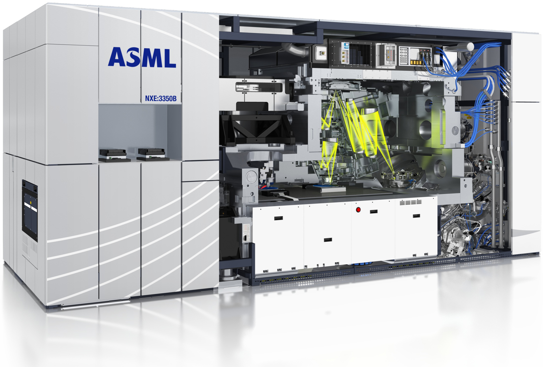
Since Samsung plans to start risk production using the 7LPP in the second half of 2018, the technology is hardly going to be used for high-volume manufacturing before the second half of 2019. Keeping in mind that Samsung now begins HVM using its leading-edge process technologies in October, it is possible that it is going to kick-off 7LPP HVM in fall 2019, but the 8LPP will be Samsung’s most advanced process technology for the better part of the year. Samsung does not mention timeframes for its 6 nm process technology and what to expect from it, but it is logical to assume that it will require more layers to be processed using ASML's EUV tools (like the NXE:3350B pictured above) in a bid to provide PPA advantages and it not be used for high-volume manufacturing before late 2020.
In March, Samsung only made brief announcements regarding its 10LPU, 8LPP and 6 nm process technology without disclosing their exact specifications or even PPA improvements targets. The addition of at least two more DUV technologies (the 10LPU and the 8LPP) in general may indicate that EUV may not be the best choice for all applications in 2019 – 2021, which is perfectly logical. Then again, we do not know how DUV and EUV technologies will co-exist early in the EUV era.
We are going to learn more about Samsung’s plans in the foundry industry in late May, when the company hosts its 2017 U.S Samsung Foundry Forum. So, we will have to wait for a couple of months for Samsung to disclose the whole picture regarding its upcoming process technologies.


89 Comments
View All Comments
mdriftmeyer - Friday, May 5, 2017 - link
Being 63.63 times smaller in diameter for an atom compared to the fab process is quite a large span in scale.boeush - Saturday, May 6, 2017 - link
One thing to consider, though, is that when atoms are bound into molecules via covalent bonds, the distances between their nuclei shrink below the sum of the adjacent atoms' stand-alone radii: in other words, chemically bound atoms pack together much more tightly than one might naively expect by conceptualizing each atom as a solid sphere...Jon Tseng - Friday, May 5, 2017 - link
PSA: NODES WITH THE SAME (NUMERICAL) NAME FROM DIFFERENT VENDORS ARE NOT EQUIVALENT.Just wanted to get that out of the way early! :-p
Meteor2 - Friday, May 5, 2017 - link
Indeed. The x nm labels are meaningless now; they may as well call them Bob and Joan.The only way to compare them is via the inter-node PPA change metrics. Anyone have numbers for 22->14 and 14->10 from Intel to hand?
Even then I know Intel's 14 nm is better on at least power and performance than others' 14/16 nm, as the latter are actually 20 nm with FinFET added, but I'm not aware of any meaningful way of comparing them.
lefty2 - Friday, May 5, 2017 - link
That's not totally true. The first iteration of Intel's 14nm performed worse than TSMC's 16nm. 14nm+ is much better thoughDrumsticks - Friday, May 5, 2017 - link
I'm not calling you wrong or anything, but can you source that? Intel's original 14nm might have had bad yields for a while, but I imagine it's difficult to compare outright performance without published numbers, given that Intel's 14nm went into CPUs with a frequency of 800MHz to 4.5 GHz, versus TSMC's biggest wins being Apple and GPUs, none of which went past the low 2GHzs. Obviously it's difficult to compare performance on frequency with something like that.SuperMecha - Saturday, May 6, 2017 - link
See page 4. There are probably several other factors that determine performance other than leakage and drive current.https://newsroom.intel.com/newsroom/wp-content/upl...
Meteor2 - Sunday, May 7, 2017 - link
Good link, and a good quote within:"Industry “10 nm” technologies are expected to ship sometime in 2017 and have similar density to Intel’s 14 nm technology that has been shipping since 2014."
helvete - Thursday, July 20, 2017 - link
Would you expect anything else from Intel paper? (Not telling they are far from the truth)lefty2 - Saturday, May 6, 2017 - link
The first iteration of 14nm was Broadfield and Broadfield did not clock to 4.5GHz. Also, you can't compare to a smartphone SoC, which have to keep within a very small power envelope.