Samsung and TSMC Roadmaps: 8 and 6 nm Added, Looking at 22ULP and 12FFC
by Anton Shilov on May 5, 2017 9:30 AM EST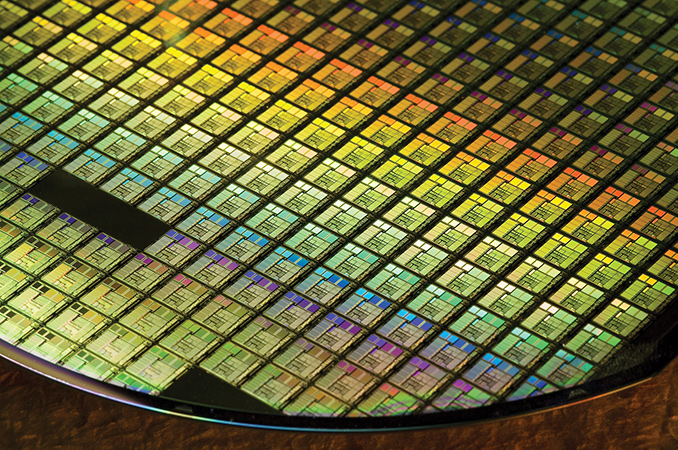
Samsung and TSMC made several important announcements about the present and future of their semiconductor manufacturing technologies in March. Samsung revealed that it had shipped over 70 thousand wafers processed using its first-generation 10 nm FinFET fabrication process (10LPE) and also announced major additions to its upcoming manufacturing technology roadmap. In particular, the company plans to introduce three processes it has not talked about thus far. TSMC said that it is about to start mass production of ICs (integrated circuits) using its first-gen 10 nm technology and also announced several new processes that will be launched in the coming years, including its first 7 nm EUV process due in 2019.
10 nm: Samsung Is Shipping
Update 5/12: Samsung informed us that its press release from October, 2016, compares characteristics of the 10LPE manufacturing technology with those of the 14LPE, not 14LPP. The text and table have been updated accordingly.
Samsung said it had started to make SoCs using its 10LPE fabrication technology last October, which is something we already knew. This manufacturing process allowed the company to make its chips 30% smaller compared to ICs made using its 14LPE process as well as reducing power consumption by 40% (at the same frequency and complexity) or increase their frequency by 27% (at the same power and complexity). So far, Samsung has processed over 70 thousand wafers using its 10LPE technology, which can give an idea about Samsung’s 10 nm production capacities (considering that the whole 10 nm production cycle is greater than the 90 days we saw with previous-gen FinFET processes). At the same time, keep in mind that Samsung does not have many 10 nm designs to manufacture right now: we know only of the company’s own Exynos 9 Octa 8895 as well as Qualcomm’s Snapdragon 835 seen in the Samsung Galaxy S8.
| Advertised PPA Improvements of New Process Technologies Data announced by companies during conference calls, press briefings and in press releases |
||||||||
| GF | Samsung | |||||||
| 7nm DUV vs 14LPP |
14LPP vs 28LPP |
10LPE vs 14LPE |
10LPE vs 14LPP |
10LPP vs 10LPE |
10LPU vs 10LPE |
|||
| Power | >60% | 60% | 40% | 30% | ~15% | ? | ||
| Performance | >30% | 40% | 27% | >10% | ~10% | ? | ||
| Area Reduction | >50% | 50% | 30% | 30% | none | ? | ||
In addition to its production milestone, Samsung also confirmed plans to start mass production of chips using its second-generation 10 nm manufacturing process called 10LPP (10 nm low-power plus) by the end of 2017 as well as its third-generation 10 nm technology called 10LPU by the end of 2018. Samsung said last year that the 10LPP is going to enable a ~10% performance increase (at the same power and at the same complexity) versus the 10LPE, but we know absolutely nothing about the 10LPU. It is logical to assume that the 10LPU will bring certain PPA-related (performance, power, area) improvements, but it is not clear how Samsung plans to achieve them and which one of the three will be the focus for improvements. As it appears, just like Intel, Samsung has ended up with three generations of 14 nm fabrication processes and is going to end up with three generations of 10 nm manufacturing technologies. It is noteworthy that Samsung itself does not use its 14LPC (low-power compact) for its leading edge SoCs, which may suggest that the 10LPU is also not aimed at this segment of the market. In fact, it is highly likely that the 10LPU will target ultra-small and ultra-low-power ICs for various emerging devices, but Samsung yet has to confirm that.
10nm: TSMC Is Steady
As for TSMC, its 10 nm process technology (CLN10FF) is now qualified for production at the company’s GigaFabs 12 and 15, where high-volume ramp is expected to start in H2 2017. Production capacity of these two fabs is hundreds of thousands wafer starts per quarter and TSMC plans to ship 400 thousand wafers processed using its 10 nm manufacturing tech this year. Considering the long production cycles for FinFET-based technologies, it is about time for TSMC to start ramping up 10 nm so to be able to supply enough chips to its main customer in time. Apple is expected to launch its new iPhone products in September or October and needs to get SoCs couple of months before the launch.
| Advertised PPA Improvements of New Process Technologies Data announced by companies during conference calls, press briefings and in press releases |
|||||||
| TSMC | |||||||
| 16FF+ vs 28HPM |
16FF+ vs 20SOC |
10FF vs 16FF+ |
7FF vs 16FF+ |
7FF vs 10FF |
|||
| Power | 70% | 60% | 40% | 60% | <40% | ||
| Performance | 65% | 40% | 20% | 30% | ? | ||
| Area Reduction | ~50% | none | >50% | 70% | >37% | ||
PPA advantages of TSMC’s CLN10FF over its CLN16FF+ (second-gen 16 nm) have been discussed already and they are significant for developers of mobile SoCs (but not that significant for makers of other ICs): a ~50% higher transistor density, a 20% performance improvement at the same power and complexity or a 40% lower power consumption at the same frequency and complexity. Unlike Samsung, TSMC does not seem to plan multiple generations of 10 nm and will go straight to 7 nm next year. 7nm is currently very popular among chip designers, indicating a future major milestone. However, in addition to the CLN7FF, the company will also offer several other manufacturing technologies for ultra-small and ultra-low-power applications.


89 Comments
View All Comments
melgross - Saturday, May 6, 2017 - link
A lot of chip experts don't believe that a true 5nm is possible. Not because we can't build it, but because the laws of physics are closing in. At that point, we have no substitute for FinFET, which doesn't work below 7 nm, and the three technologies that have been considered as a replacement aren't working either.When you begin to have features that are just 10 to 12 atoms wide, Heisenberg's Law hits you hard. As many electrons that travel through the feature, escape it. That's a death hell. So I expect that 7nm will really be 10 to 14 for most fabs, the way 14 is really 16 to 20 for most now.
The next step is expected to be carbon nanotubes, which both Hp and ibm have been working for years, and have shown limited success. That hoped to be ready, in limited complexity, by 2005 to 2030.
But there will be a wide gap between any silicon technology and that, even assuming they can get it working on a commercial basis at all. There are still too many steps for that, and they don't yet know how to climb them, or even if they're there.
melgross - Saturday, May 6, 2017 - link
Oops, too many typos. I meant, ready by 2025 to 2030, of course.Meteor2 - Sunday, May 7, 2017 - link
You're right, but I think between EUV and further development of the new gate concepts we'll make 5 nm happen. Although as really it's a question of whether commercial interests will fund the R&D, rather can 'science' make it happen, I suppose there's a risk 5 nm won't happen as designing such chips will be fantastically expensive. Will we be prepared to spend the $$$ for the performance which would be delivered?lefty2 - Friday, May 5, 2017 - link
Intel already has lost it's process advantage. Samsung's 10nm is currently in HVM and denser than Intel's 14nm. Intel say they will launch 10nm in 2017, but the yields are so bad they can hardly be considered production yield. By the time it reaches production yield TSMC will have 7nmDrumsticks - Friday, May 5, 2017 - link
Intel's 10nm is going to be denser than Samsung or TSMC's 7nm imo, going by the numbers we see here. Intel's 14nm is already denser than their competition by somewhere in the realm of 30% (per the hard numbers Intel released a few weeks back, and nobody has contradicted them). Intel's jump to 10nm is going to provide ~2.7x higher density than their 14nm node, and I think they've said several times they plan to ship 10nm this year.Even with a 70% area reduction on 7nm vs 16nm at TSMC, I don't think that overcomes a 30% lead + a 2.7x increase in density on top of that lead.
For another comparison, Intel's 10nm measures 100M transistors / mm^2, versus their competition at 50M / mm^2 at 10nm. Assuming TSMC's transistor density is around the "Others" metric, a 37% reduction in area from 10nm to 7nm would still leave them short of Intel's process node. I suspect everybody else will need a 5nm node to temporarily jump ahead of Intel's 10nm, before Intel's 7nm rolls around in 2020 or something and puts everybody behind again.
Numbers come from https://newsroom.intel.com/newsroom/wp-content/upl... which based on most of what I've seen has been accepted as a well done report. I'd love to see everybody switch to a more objective metric, since process node is now just a marketing game.
vladx - Friday, May 5, 2017 - link
They obviously can't compete with Intel head-to-head so say they have to resort to marketing gimmicks to make it appear they're coming ahead.SuperMecha - Saturday, May 6, 2017 - link
Intel's 14nm density advantage compared to GF/Samsung's 14nm process is only 23% not 30%. Also Intel's recent presentation only compares up to their competitor's 10nm not 7nm. In 2018 Intel will lose it transistor density advantage.https://www.semiwiki.com/forum/content/6713-14nm-1...
Drumsticks - Saturday, May 6, 2017 - link
I know Intel compared to the 10nm products; I was just extrapolating from that based on what TSMC stated (in the article) about their 7nm vs their own 16nm and 10nm. With everybody using different statistics now for each of their parts, it's not surprising that Intel gets passed every now and then, considering the time between their nodes is getting longer and longer.lefty2 - Saturday, May 6, 2017 - link
Scotten Jones did a detailed analysis of various leading edge nodes and concluded that TSMC's 7nm is slightly denser than Intel's 10nm and Samsun/TSMC 10nm is slightly desnser than Intel's 14nm:https://www.semiwiki.com/forum/content/6713-14nm-1...
Intel's 2017 launch of 10nm is virtually a paper launch. They are only going to release a couple of low volume SKUs at the very end of 2017, just so they can claim that they have the process lead. It's not till late 2018, or 2019 that the bulk of their products go to 10nm. Also the first iteration of 10nm performs worse than Intel's current 14nm+ process.
melgross - Saturday, May 6, 2017 - link
I don't believe it. First of all, neither he, or anyone else outside those companies actually knows enough about the actual chips to know the true density. Evaluating these by making some basic mathematical calculations doesn't tell us anything about the actual processes. It's all theoretical.