Samsung and TSMC Roadmaps: 8 and 6 nm Added, Looking at 22ULP and 12FFC
by Anton Shilov on May 5, 2017 9:30 AM ESTBeyond 10 nm at Samsung: 8 nm and 6 nm
Samsung’s 7 nm manufacturing technology is still expected to be the company’s first process to use extreme ultraviolet lithography (EUVL) for high-volume manufacturing (HVM) and that is going to happen sometimes in 2019 or later (risk production starts in the second half of 2018). In fact, the next several years down the road is where things will start to get interesting as Samsung announced another two new production technologies it has not talked about before: the 8 nm and the 6 nm processes.
| Industry FinFET Lithography Roadmap, HVM Start Data announced by companies during conference calls, press briefings and in press releases |
||||||||||||
| 2016 | 2017 | 2018 | 2019 | 2020 | 2021 | |||||||
| 1H | 2H | 1H | 2H | 1H | 2H | 1H | 2H | |||||
| GlobalFoundries | 14LPP | 7nm DUV | 7nm with EUV* | |||||||||
| Intel | 14 nm 14 nm+ |
14 nm++ 10 nm |
10 nm+ 10 nm++ |
|||||||||
| Samsung | 14LPP 14LPC |
10LPE | 10LPP | 8LPP 10LPU |
7LPP | 6 nm* (?) | ||||||
| SMIC | 28 nm** | 14 nm in development | ||||||||||
| TSMC | CLN16FF+ CLN16FFC | CLN10FF CLN16FFC |
CLN7FF CLN12FFC |
CLN12FFC/ CLN12ULP |
CLN7FF+ | 5 nm* (?) | ||||||
| UMC | 28 nm** | 14nm | no data | |||||||||
| *Exact timing not announced **Planar |
||||||||||||
Officially, Samsung says that both technologies will offer “greater scalability, performance and power advantages when compared to existing process nodes,” which obviously means that they are across the board better than Samsung’s current-gen 14 nm and 10 nm offerings. What is important is that Samsung also says that the “8 nm and the 6 nm will inherit all innovations from the latest 10 nm and the 7 nm technologies” respectively. This means that the 8 nm is set to keep using DUV and multi patterning (triple patterning or even quad patterning to be exact, but Samsung has not confirmed usage of the latter) for critical layers, whereas the 6 nm will come after 7 nm and will be Samsung’s second-generation EUV technology.
The only thing that Samsung confirms about its 8LPP manufacturing technology right now is the fact that this is a DUV-based process technology designed to shrink die size (i.e., increase transistor density) and frequency compared to the 10LPP fabrication process. Given the name of the technology and its key advertised advantages over direct predecessor, it is highly likely that the 8LPP will be used to make high-performance SoCs in 2019.
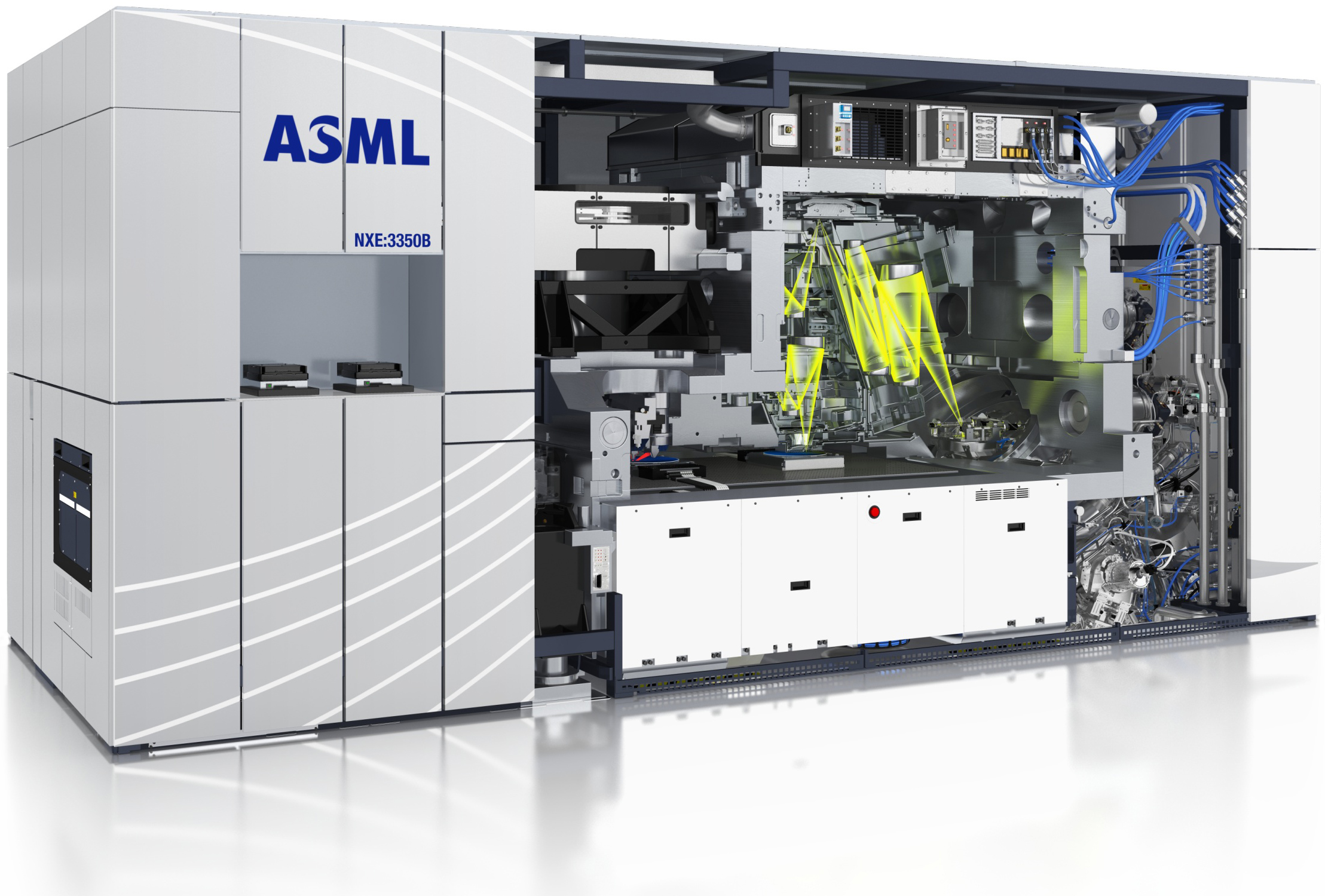
Since Samsung plans to start risk production using the 7LPP in the second half of 2018, the technology is hardly going to be used for high-volume manufacturing before the second half of 2019. Keeping in mind that Samsung now begins HVM using its leading-edge process technologies in October, it is possible that it is going to kick-off 7LPP HVM in fall 2019, but the 8LPP will be Samsung’s most advanced process technology for the better part of the year. Samsung does not mention timeframes for its 6 nm process technology and what to expect from it, but it is logical to assume that it will require more layers to be processed using ASML's EUV tools (like the NXE:3350B pictured above) in a bid to provide PPA advantages and it not be used for high-volume manufacturing before late 2020.
In March, Samsung only made brief announcements regarding its 10LPU, 8LPP and 6 nm process technology without disclosing their exact specifications or even PPA improvements targets. The addition of at least two more DUV technologies (the 10LPU and the 8LPP) in general may indicate that EUV may not be the best choice for all applications in 2019 – 2021, which is perfectly logical. Then again, we do not know how DUV and EUV technologies will co-exist early in the EUV era.
We are going to learn more about Samsung’s plans in the foundry industry in late May, when the company hosts its 2017 U.S Samsung Foundry Forum. So, we will have to wait for a couple of months for Samsung to disclose the whole picture regarding its upcoming process technologies.


89 Comments
View All Comments
vladx - Friday, May 5, 2017 - link
Yep I'm skeptical about a software development revolution, I think focusing on better computer architectures has a much better outlook.melgross - Saturday, May 6, 2017 - link
Well, there's the question of whether we can get a revolutionary computer architecture these days. It not easy. So we're still looking at cisc vs risc. Maybe we need to go more risc and less cisc. Pretty much everything is some combo of the two.ABR - Sunday, May 7, 2017 - link
No revolution, but technology has been and will continue advancing here for a long time. Higher-level languages and object-oriented programming making larger projects possible. Evolution in UI frameworks and asynchronous programming (cutting edge in mobile frameworks). Hardware virtualization, network definition migrating to software, and environment encapsulation (e.g., Docker), simplifying resource management. Frameworks like OpenGL, EX, Metal bridging the gap between graphics and graphics hardware. Libraries like Caffe and TensorFlow doing the same for neural networks and learning software.Also engineering tools and techniques. Distributed version control systems for source code management. Suites like dpkg or maven for handling dependencies. Team and process practices like the family of Agile techniques.
The sophistication and sheer amount and ubiquity of software applications in our lives today depends just as much on all of these things as on faster, lower power hardware.
boeush - Saturday, May 6, 2017 - link
Once we reach the absolute quantum limits of 2d scaling, we will be looking at alternative materials (graphene, nanotubes, diamond, III-IV chemistry, etc) for better power and frequency scaling. At the same time, 3D stacking of 2D layers by the dozens, then hundreds, then thousands. At the same time, advanced heat dissipation tech (graphene/nanotubes/diamond could serve double duty there), as well as (at least for non-portable devices) refrigeration not just for overclocking but for normal operation. Maybe even look into superconducting chips/interconnects using high-Tc materials, immersed in liquid Nitrogen... There's also research into molecular computing. And, of course, you can always trade off generality against special purpose accelerator ASICs that can provide many-orders-of-magnitude speedup vs conventional processors on same node in specific tasks: and the more compact the node, the more of these various narrow-use circuits you can affordably cram onto a single chip...melgross - Saturday, May 6, 2017 - link
Sure, there are a lot of technologies out there. But most are just impractical, or just too expensive, and complex. We've has liquid cooling for some time, but do most people really want that? What about notebooks? Can't really be done.Other technologies have been considered for a couple of decades but as so expensive that envelope mainframe CPUs can't use them.
Most of these technologies can be used for every high end use, because of expense, effectiveness, and even power draw. But that's just for the top 0.1% of computing. What about the rest of us?
ironargonaut - Monday, May 8, 2017 - link
You mean like when they said that the physics of light would prevent any geometries less then 193nm? Sorry, but the "wall" that was going to end CPU density increases has been broken so many times, that I won't believe it till I see it. Of course just because all those predictions where wrong doesn't mean yours is. Cheers.Gich - Friday, May 5, 2017 - link
Some time ago I dig up this:"14/16nm":
Intel ~13.4nm - from Broadwell to Coffee Lake, Atom x5/x7
Samsung/GFo ~16.6nm - AMD Zen and Rx400/500, nVidia 1050, SD 620/820, Exynos 7/8, Apple A9
TSMC ~18.3nm - nVidia 1060+, Apple A9/10
"10nm":
Intel ~9.5nm - Cannonlake
TSMC ~11.3nm - Helio X30, Kirin 970, Apple A10X
Samsung ~12.0nm - SD835, Exynos 9
Gich - Friday, May 5, 2017 - link
"7nm":Intel ~6.7nm
TSMC/GF ~8.2nm
Samsung ~8.4nm
smalM - Monday, May 8, 2017 - link
TSMC ~18.3nm - that's 16FF which was never used for mass production but is always used by Intel for comparison...helvete - Thursday, July 20, 2017 - link
Intel paper, intel's point of view.