Samsung and TSMC Roadmaps: 8 and 6 nm Added, Looking at 22ULP and 12FFC
by Anton Shilov on May 5, 2017 9:30 AM EST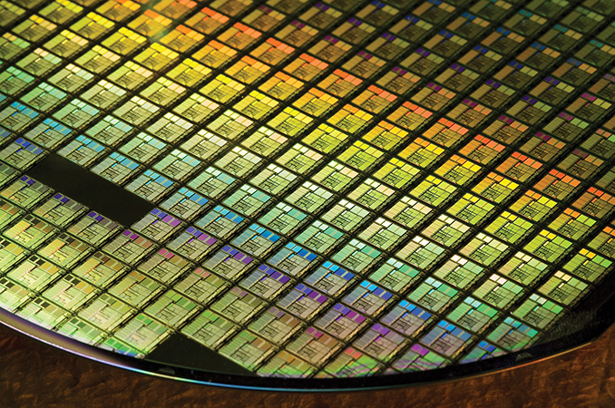
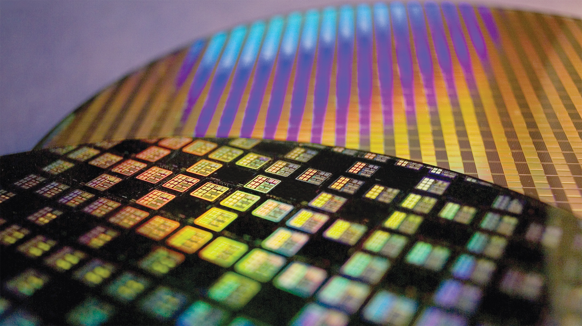
Samsung and TSMC made several important announcements about the present and future of their semiconductor manufacturing technologies in March. Samsung revealed that it had shipped over 70 thousand wafers processed using its first-generation 10 nm FinFET fabrication process (10LPE) and also announced major additions to its upcoming manufacturing technology roadmap. In particular, the company plans to introduce three processes it has not talked about thus far. TSMC said that it is about to start mass production of ICs (integrated circuits) using its first-gen 10 nm technology and also announced several new processes that will be launched in the coming years, including its first 7 nm EUV process due in 2019.
10 nm: Samsung Is Shipping
Update 5/12: Samsung informed us that its press release from October, 2016, compares characteristics of the 10LPE manufacturing technology with those of the 14LPE, not 14LPP. The text and table have been updated accordingly.
Samsung said it had started to make SoCs using its 10LPE fabrication technology last October, which is something we already knew. This manufacturing process allowed the company to make its chips 30% smaller compared to ICs made using its 14LPE process as well as reducing power consumption by 40% (at the same frequency and complexity) or increase their frequency by 27% (at the same power and complexity). So far, Samsung has processed over 70 thousand wafers using its 10LPE technology, which can give an idea about Samsung’s 10 nm production capacities (considering that the whole 10 nm production cycle is greater than the 90 days we saw with previous-gen FinFET processes). At the same time, keep in mind that Samsung does not have many 10 nm designs to manufacture right now: we know only of the company’s own Exynos 9 Octa 8895 as well as Qualcomm’s Snapdragon 835 seen in the Samsung Galaxy S8.
| Advertised PPA Improvements of New Process Technologies Data announced by companies during conference calls, press briefings and in press releases |
||||||||
| GF | Samsung | |||||||
| 7nm DUV vs 14LPP |
14LPP vs 28LPP |
10LPE vs 14LPE |
10LPE vs 14LPP |
10LPP vs 10LPE |
10LPU vs 10LPE |
|||
| Power | >60% | 60% | 40% | 30% | ~15% | ? | ||
| Performance | >30% | 40% | 27% | >10% | ~10% | ? | ||
| Area Reduction | >50% | 50% | 30% | 30% | none | ? | ||
In addition to its production milestone, Samsung also confirmed plans to start mass production of chips using its second-generation 10 nm manufacturing process called 10LPP (10 nm low-power plus) by the end of 2017 as well as its third-generation 10 nm technology called 10LPU by the end of 2018. Samsung said last year that the 10LPP is going to enable a ~10% performance increase (at the same power and at the same complexity) versus the 10LPE, but we know absolutely nothing about the 10LPU. It is logical to assume that the 10LPU will bring certain PPA-related (performance, power, area) improvements, but it is not clear how Samsung plans to achieve them and which one of the three will be the focus for improvements. As it appears, just like Intel, Samsung has ended up with three generations of 14 nm fabrication processes and is going to end up with three generations of 10 nm manufacturing technologies. It is noteworthy that Samsung itself does not use its 14LPC (low-power compact) for its leading edge SoCs, which may suggest that the 10LPU is also not aimed at this segment of the market. In fact, it is highly likely that the 10LPU will target ultra-small and ultra-low-power ICs for various emerging devices, but Samsung yet has to confirm that.
10nm: TSMC Is Steady
As for TSMC, its 10 nm process technology (CLN10FF) is now qualified for production at the company’s GigaFabs 12 and 15, where high-volume ramp is expected to start in H2 2017. Production capacity of these two fabs is hundreds of thousands wafer starts per quarter and TSMC plans to ship 400 thousand wafers processed using its 10 nm manufacturing tech this year. Considering the long production cycles for FinFET-based technologies, it is about time for TSMC to start ramping up 10 nm so to be able to supply enough chips to its main customer in time. Apple is expected to launch its new iPhone products in September or October and needs to get SoCs couple of months before the launch.
| Advertised PPA Improvements of New Process Technologies Data announced by companies during conference calls, press briefings and in press releases |
|||||||
| TSMC | |||||||
| 16FF+ vs 28HPM |
16FF+ vs 20SOC |
10FF vs 16FF+ |
7FF vs 16FF+ |
7FF vs 10FF |
|||
| Power | 70% | 60% | 40% | 60% | <40% | ||
| Performance | 65% | 40% | 20% | 30% | ? | ||
| Area Reduction | ~50% | none | >50% | 70% | >37% | ||
PPA advantages of TSMC’s CLN10FF over its CLN16FF+ (second-gen 16 nm) have been discussed already and they are significant for developers of mobile SoCs (but not that significant for makers of other ICs): a ~50% higher transistor density, a 20% performance improvement at the same power and complexity or a 40% lower power consumption at the same frequency and complexity. Unlike Samsung, TSMC does not seem to plan multiple generations of 10 nm and will go straight to 7 nm next year. 7nm is currently very popular among chip designers, indicating a future major milestone. However, in addition to the CLN7FF, the company will also offer several other manufacturing technologies for ultra-small and ultra-low-power applications.


89 Comments
View All Comments
Lodix - Friday, May 5, 2017 - link
Samsung's 10nmLPP has a 15% reduction in power consumption compared to the LPE version.Also the 10nmLPE numbers about performance and power 27/40% are compared to the previous 14nmLPE not the Plus version.
Lodix - Friday, May 5, 2017 - link
And the 10nmLPU version is aimed to Area reduction.Anton Shilov - Friday, May 5, 2017 - link
Thank you for the corrections. You are right about the 10LPP, they made and appropriate announcement a couple of weeks ago, but somehow I've missed it. Fixed.Regarding the 10LPE vs 14LP*, I am not sure.
They state the following:
"Samsung’s new 10nm FinFET process (10LPE) adopts an advanced 3D transistor structure with additional enhancements in both process technology and design enablement compared to its 14nm predecessor, allowing up to 30-percent increase in area efficiency with 27-percent higher performance or 40-percent lower power consumption."
http://www.anandtech.com/show/10765/samsung-10nm-m...
If you look at the picture there (http://images.anandtech.com/doci/10765/dac.png), they mention ~30% performance increase at the same leakage power, which can considered as 27%... But if you happen to see some more up to date slides from Samsung, please link them.
As for the 10LPU, I guess, they are going to make an announcement in late May.
Lodix - Friday, May 5, 2017 - link
I see the arrow joining the 14nmLPE version with 10nmLPE.Lodix - Saturday, May 6, 2017 - link
In this pdf from Samsung they specified that the improvements stated are from 14nmLPE and not from 14nmLPP.https://www.semiwiki.com/forum/attachments/f293/18...
MajGenRelativity - Friday, May 5, 2017 - link
I know AMD will be using GF 7nm for their GPUs after Vega 10/11, but I wonder what NVIDIA will be using after this current Pascal generation. Does anyone have any clues?haukionkannel - Friday, May 5, 2017 - link
If They Are vice They use at least two different distributors just like Apple.melgross - Saturday, May 6, 2017 - link
Apple has moved away from that model. I doubt they wanted to do it, but neither Samsung nor TSMC could produce all the SoCs they needed that year, so they had to.It's also interesting to note that while Apple had to tune their designs to both processes, the TSMC 16nm was 20% more efficient than the Samsung 14nm process. We saw results of those tests either here or on arstechnica, I don't remember which now. But the total device efficiency advantage was under 5% once everything was taken together.
But still, it shows that we can't go by theory when extrapolating these supposed numbers to the real world. I'd still rather see Apple on intel.
The_Assimilator - Friday, May 5, 2017 - link
I would be extremely surprised if it was anyone except TSMC. Especially since TSMC has just announced 10nm is ready for H2 this year - which, not coincidentally, is when NVIDIA is rumoured to drop the first Volta products.The only GPU that NVIDIA has ever sourced from a company other than TSMC is GP107 from Samsung at 14nm. Even though Sammy's 14nm node is worse than TSMC's 16nm, GP107 is such a (relatively) small and simple chip that it didn't really matter. We'll probably see a similar story with Volta: TSMC gets the big Pascals, Samsung gets the small ones.
There is, of course, always the possibility that NVIDIA will stick with the now-mature (and cheaper) 16nm for Volta - I imagine it will depend on whether Volta is more (10nm) or less (16nm) powerful clock-for-clock compared to Pascal.
Kevin G - Sunday, May 7, 2017 - link
nVidia has been flirting with Samsung of late. I doubt they'd just exclusively to Samsung but they'll likely continue to have small/medium chip there as a testing vehicle if they need to quickly switch their entire line up over.