Samsung and TSMC Roadmaps: 8 and 6 nm Added, Looking at 22ULP and 12FFC
by Anton Shilov on May 5, 2017 9:30 AM EST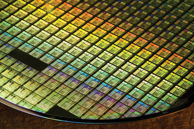
Samsung and TSMC made several important announcements about the present and future of their semiconductor manufacturing technologies in March. Samsung revealed that it had shipped over 70 thousand wafers processed using its first-generation 10 nm FinFET fabrication process (10LPE) and also announced major additions to its upcoming manufacturing technology roadmap. In particular, the company plans to introduce three processes it has not talked about thus far. TSMC said that it is about to start mass production of ICs (integrated circuits) using its first-gen 10 nm technology and also announced several new processes that will be launched in the coming years, including its first 7 nm EUV process due in 2019.
10 nm: Samsung Is Shipping
Update 5/12: Samsung informed us that its press release from October, 2016, compares characteristics of the 10LPE manufacturing technology with those of the 14LPE, not 14LPP. The text and table have been updated accordingly.
Samsung said it had started to make SoCs using its 10LPE fabrication technology last October, which is something we already knew. This manufacturing process allowed the company to make its chips 30% smaller compared to ICs made using its 14LPE process as well as reducing power consumption by 40% (at the same frequency and complexity) or increase their frequency by 27% (at the same power and complexity). So far, Samsung has processed over 70 thousand wafers using its 10LPE technology, which can give an idea about Samsung’s 10 nm production capacities (considering that the whole 10 nm production cycle is greater than the 90 days we saw with previous-gen FinFET processes). At the same time, keep in mind that Samsung does not have many 10 nm designs to manufacture right now: we know only of the company’s own Exynos 9 Octa 8895 as well as Qualcomm’s Snapdragon 835 seen in the Samsung Galaxy S8.
| Advertised PPA Improvements of New Process Technologies Data announced by companies during conference calls, press briefings and in press releases |
||||||||
| GF | Samsung | |||||||
| 7nm DUV vs 14LPP |
14LPP vs 28LPP |
10LPE vs 14LPE |
10LPE vs 14LPP |
10LPP vs 10LPE |
10LPU vs 10LPE |
|||
| Power | >60% | 60% | 40% | 30% | ~15% | ? | ||
| Performance | >30% | 40% | 27% | >10% | ~10% | ? | ||
| Area Reduction | >50% | 50% | 30% | 30% | none | ? | ||
In addition to its production milestone, Samsung also confirmed plans to start mass production of chips using its second-generation 10 nm manufacturing process called 10LPP (10 nm low-power plus) by the end of 2017 as well as its third-generation 10 nm technology called 10LPU by the end of 2018. Samsung said last year that the 10LPP is going to enable a ~10% performance increase (at the same power and at the same complexity) versus the 10LPE, but we know absolutely nothing about the 10LPU. It is logical to assume that the 10LPU will bring certain PPA-related (performance, power, area) improvements, but it is not clear how Samsung plans to achieve them and which one of the three will be the focus for improvements. As it appears, just like Intel, Samsung has ended up with three generations of 14 nm fabrication processes and is going to end up with three generations of 10 nm manufacturing technologies. It is noteworthy that Samsung itself does not use its 14LPC (low-power compact) for its leading edge SoCs, which may suggest that the 10LPU is also not aimed at this segment of the market. In fact, it is highly likely that the 10LPU will target ultra-small and ultra-low-power ICs for various emerging devices, but Samsung yet has to confirm that.
10nm: TSMC Is Steady
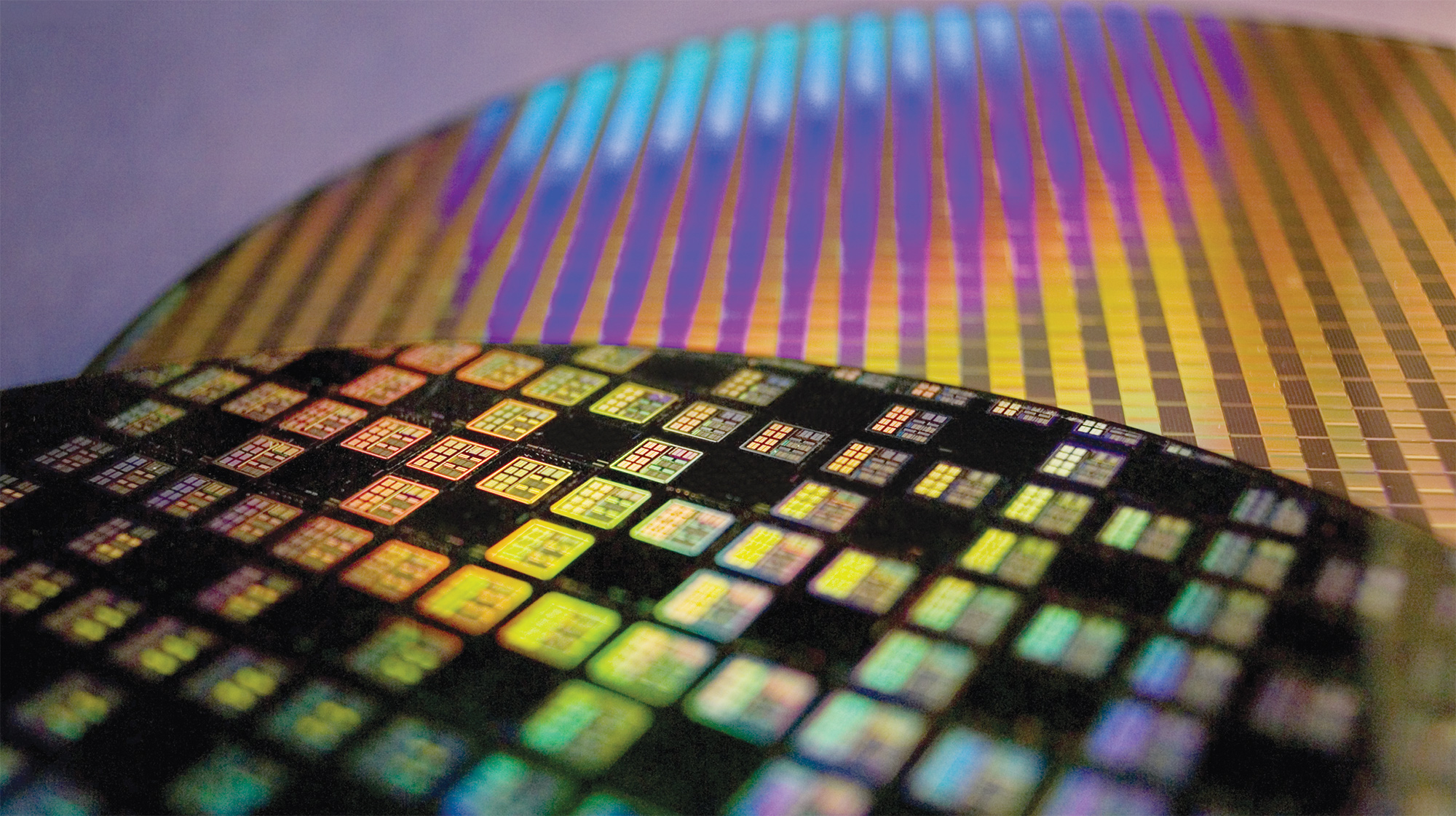
As for TSMC, its 10 nm process technology (CLN10FF) is now qualified for production at the company’s GigaFabs 12 and 15, where high-volume ramp is expected to start in H2 2017. Production capacity of these two fabs is hundreds of thousands wafer starts per quarter and TSMC plans to ship 400 thousand wafers processed using its 10 nm manufacturing tech this year. Considering the long production cycles for FinFET-based technologies, it is about time for TSMC to start ramping up 10 nm so to be able to supply enough chips to its main customer in time. Apple is expected to launch its new iPhone products in September or October and needs to get SoCs couple of months before the launch.
| Advertised PPA Improvements of New Process Technologies Data announced by companies during conference calls, press briefings and in press releases |
|||||||
| TSMC | |||||||
| 16FF+ vs 28HPM |
16FF+ vs 20SOC |
10FF vs 16FF+ |
7FF vs 16FF+ |
7FF vs 10FF |
|||
| Power | 70% | 60% | 40% | 60% | <40% | ||
| Performance | 65% | 40% | 20% | 30% | ? | ||
| Area Reduction | ~50% | none | >50% | 70% | >37% | ||
PPA advantages of TSMC’s CLN10FF over its CLN16FF+ (second-gen 16 nm) have been discussed already and they are significant for developers of mobile SoCs (but not that significant for makers of other ICs): a ~50% higher transistor density, a 20% performance improvement at the same power and complexity or a 40% lower power consumption at the same frequency and complexity. Unlike Samsung, TSMC does not seem to plan multiple generations of 10 nm and will go straight to 7 nm next year. 7nm is currently very popular among chip designers, indicating a future major milestone. However, in addition to the CLN7FF, the company will also offer several other manufacturing technologies for ultra-small and ultra-low-power applications.


89 Comments
View All Comments
Azethoth - Friday, May 5, 2017 - link
This is exciting news. The existence of GigaFabs means we must be getting close to the first MegaFab!ishould - Friday, May 5, 2017 - link
You mean TeraFab?LuckyWhale - Tuesday, May 9, 2017 - link
I wish Anton would work more on his writing or get a better editor. He writes English so mechanically and itis painfully obvious English is nowhere near his first tongue. I used to follow him at Xbitlabs. Great content but poor writing! sorry.ABR - Thursday, May 11, 2017 - link
Hmm, normally I'm a stickler about this stuff but with Anton's articles I guess I'm usually so immersed in the content that I don't notice anything!nhisaka - Tuesday, May 9, 2017 - link
In lịch tết 2018 : http://thietkelichtet.vn/bang-gia-in-lich-tet-bang...Thiet ke biet thu: http://katahome.com/thiet-ke-biet-thu
darkich - Wednesday, May 10, 2017 - link
Soo..no 7nm on Intel's roadmap?Seems like Samsung, GF and TSMC are on their way to leave it in the dust
peevee - Friday, May 12, 2017 - link
The "nodes" are just pure lies at this point. 45nm doubled gate density of 65nm, as expected. 10nm chips should have 20 times more transistors per area unit compared to 45nm. They are not even close. And there is nothing which is really 10nm, even a feature as simple as metal pitch is 40-50nm.RubiNBA - Monday, May 15, 2017 - link
The NBA live mobile Online additionally help gamers earn coins that are easy and quick. Since the primary resources in the game is coins, players that have use of unlimited coins have better opportunity to win the game as well as at a short time that is considerable.
Source : http://ow.ly/AHwi30aK5bD
thuantruongadw - Saturday, July 22, 2017 - link
Đất nền Long Hưng https://khudothi-longhung.comKhu đô thị Long Hưng https://khudothi-longhung.com/tien-ich-khu-do-thi-...
Đất nền long hưng giá rẻ nên đầu tư ngay https://datnenvensong.info/