NVIDIA Volta Unveiled: GV100 GPU and Tesla V100 Accelerator Announced
by Ryan Smith on May 10, 2017 5:00 PM EST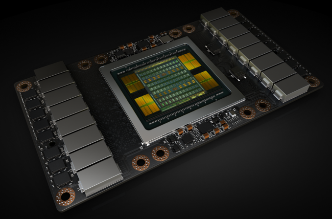
Today at their annual GPU Technology Conference keynote, NVIDIA's CEO Jen-Hsun Huang announced the company's first Volta GPU and Volta products. Taking aim at the very high end of the compute market with their first products, NVIDIA has laid out a very aggressive technology delivery schedule in order to bring about another major leap in GPU deep learning performance.
As a quick history lesson, NVIDIA first unveiled the Volta architecture name all the way back in 2013. What eventually happened with their architectures wasn’t what was originally announced – Maxwell and Volta became Maxwell, Pascal, and Volta – but Volta is the last GPU architecture on NVIDIA’s current public roadmap. Until now, all we’ve known about Volta is that it existed; NVIDIA has opted to focus on what’s directly in front of them (e.g. Pascal), one generation at a time.
So let’s talk Volta. For their first Volta products, NVIDIA is following a very similar path as they did with Pascal last year. Which is to say that they are kicking off their public campaign and product stack with a focus on business, HPC, and deep learning, rather than consumer GPUs. Volta is a full GPU architecture for both compute and graphics, but today’s announcements are all about the former. So the features unveiled today and as part of the first Volta GPU are all compute-centric.
NVIDIA’s first Volta GPU then is the aptly named GV100. The successor to the Pascal GP100, this is NVIDIA’s flagship GPU for compute, designed to drive the next generation of Tesla products.
| NVIDIA GPU Specification Comparison | |||||
| GV100 | GP100 | GK110 | |||
| CUDA Cores | 5376 | 3840 | 2880 | ||
| Tensor Cores | 672 | N/A | N/A | ||
| SMs | 84 | 60 | 15 | ||
| CUDA Cores/SM | 64 | 64 | 192 | ||
| Tensor Cores/SM | 8 | N/A | N/A | ||
| Texture Units | 336 | 240 | 240 | ||
| Memory | HBM2 | HBM2 | GDDR5 | ||
| Memory Bus Width | 4096-bit | 4096-bit | 384-bit | ||
| Shared Memory | 128KB, Configurable | 24KB L1, 64KB Shared | 48KB | ||
| L2 Cache | 6MB | 4MB | 1.5MB | ||
| Half Precision | 2:1 (Vec2) | 2:1 (Vec2) | 1:1 | ||
| Double Precision | 1:2 | 1:2 | 1:3 | ||
| Die Size | 815mm2 | 610mm2 | 552mm2 | ||
| Transistor Count | 21.1B | 15.3B | 7.1B | ||
| TDP | 300W | 300W | 235W | ||
| Manufacturing Process | TSMC 12nm FFN | TSMC 16nm FinFET | TSMC 28nm | ||
| Architecture | Volta | Pascal | Kepler | ||
Before we kick things off, one thing to make clear here - and this is something that I'll get into much greater detail when NVIDIA releases enough material for a proper deep dive - is that Volta is a brand new architecture for NVIDIA in almost every sense of the word. While the internal organization is the same much of the time, it's not Pascal at 12nm with new cores (Tensor Cores). Rather it's a significantly different architecture in terms of thread execution, thread scheduling, core layout, memory controllers, ISA, and more. And these are just the things NVIDIA is willing to talk about, never mind the ample secrets they still keep. So while I can only scratch the surface for today's reveal and will be focusing on basic throughput, Volta has a great deal going on under the hood to get to in the coming weeks.
But starting with the raw specficiations, the GV100 is something I can honestly say is a audacious GPU, an adjective I’ve never had a need to attach to any other GPU in the last 10 years. In terms of die size and transistor count, NVIDIA is genuinely building the biggest GPU they can get away with: 21.1 billion transistors, at a massive 815mm2, built on TSMC’s still green 12nm “FFN” process (the ‘n’ stands for NVIDIA; it’s a customized higher perf version of 12nm for NVIDIA).
To put this in perspective, NVIDIA’s previous record holder for GPU size was GP100 at 610mm2. So GV100, besides being on a newer generation process, is a full 33% larger. In fact NVIDIA has gone right to the reticle size of TSMC’s process; GV100 is as big a GPU as the fab can build. Now NVIDIA is not a stranger with reticle sizes, as GM200 happened to do the same thing with TSMC’s 28nm process, but at only 601mm2, GV100 is much larger still.
Now why the focus on die size first and foremost? At a high level, die size correlates well with performance. But more significantly, this is a very visible flag about how NVIDIA is pushing the envelope. The company is not discussing chip yields at this time, but such a large chip is going to yield very poorly, especially on the new 12nm FFN process. NVIDIA is going to be sacrificing a lot of silicon for a relatively small number of good chips, just so that they can sell them to eager customers who are going to pay better than $15K/chip. This is how badly NVIDIA’s customers want more powerful GPUs, and how hard NVIDIA is going to push the limits of modern fab technology to deliver it.
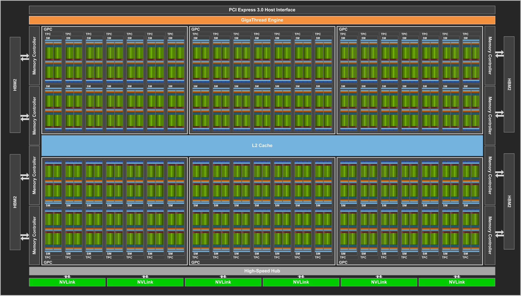
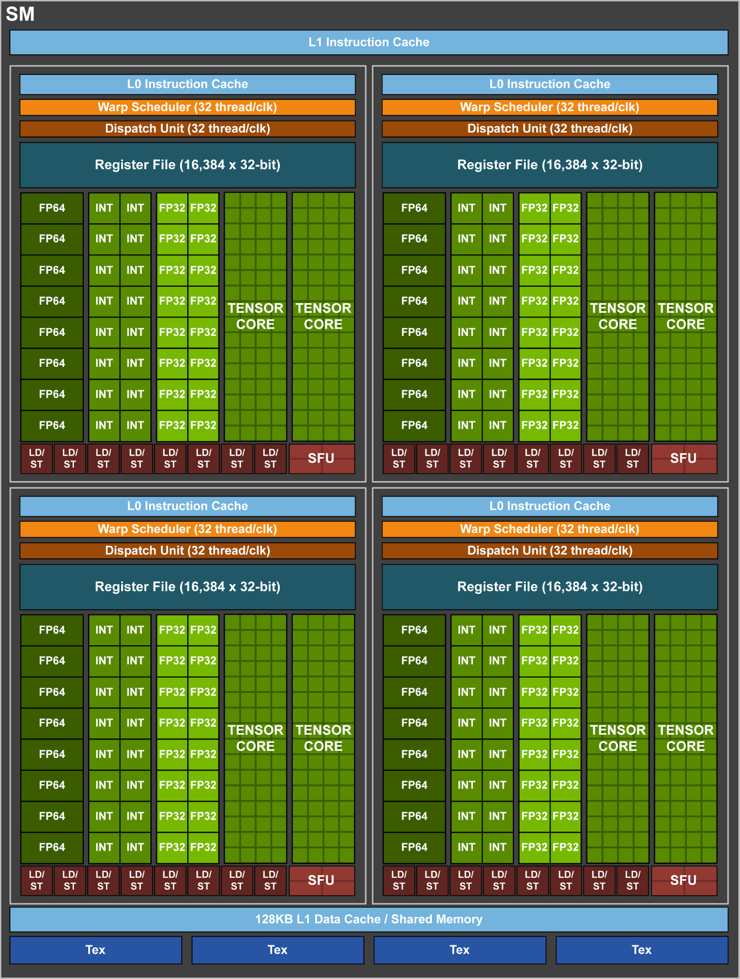
The chip’s absurd size aside, GV100 promises to be powerful. The chip contains 84 SMs – as this is a compute product, each SM is 64 CUDA cores in size – making for a total of 5376 FP32 CUDA cores. Joining those FP32 cores are 2688 FP64 CUDA cores (meaning NV is maintaining their 1:2 FP64 ratio), but also a new core that NVIDIA is calling the Tensor Core.
Tensor Cores are a new type of core for Volta that can, at a high level, be thought of as a more rigid, less flexible (but still programmable) core geared specifically for Tensor deep learning operations. These cores are essentially a mass collection of ALUs for performing 4x4 Matrix operations; specifically a fused multiply add (A*B+C), multiplying two 4x4 FP16 matrices together, and then adding that result to an FP16 or FP32 4x4 matrix to generate a final 4x4 FP32 matrix.
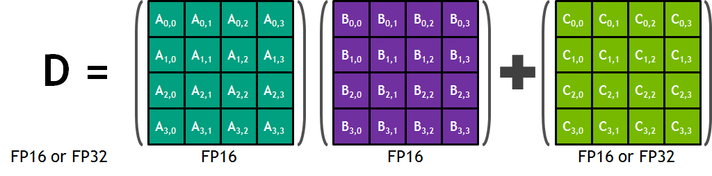
The significance of these cores are that by performing a massive matrix-matrix multiplication operation in one unit, NVIDIA can achieve a much higher number of FLOPS for this one operation. A single Tensor Core performs the equivalent of 64 FMA operations per clock (for 128 FLOPS total), and with 8 such cores per SM, 1024 FLOPS per clock per SM. By comparison, even with pure FP16 operations, the standard CUDA cores in an SM only generate 256 FLOPS per clock. So in scenarios where these cores can be used, NV is slated to be able to deliver 4x the performance versus Pascal.
Now there are a bunch of unknowns here, including how flexible these cores are, and how much die space that they take up versus FP32 CUDA cores. But at a high level, this is looking like a relatively rigid core, which would make it very die-space efficient. By lumping together so many ALUs within a single core and without duplicating their control logic or other supporting hardware, the percentage of transistors in a core dedicated to ALUs is higher than on a standard CUDA core. The cost is flexibility, as the hardware to enable flexibility takes up space. So this is a very conscious tradeoff on NVIDIA’s part between flexibility and total throughput.
Continuing down the spec list, each SM contains 4 texture units, the same number as with the GP100. Joining those texture units is yet another rework of NVIDIA’s L1 cache/shared memory architecture. Whereas GP100 had a 24KB L1/Texture cache and 64KB shared memory per SM, on GV100 it’s now a 128KB of L1 data cache/shared memory per SM, with the precise L1/shared memory split being configurable. Besides unifying these caches, this means there’s more cache/memory overall, 40KB more per SM. On the other hand, the register file remains unchanged at 256KB of registers (4x16K 32-bit registers) per SM.
At a higher level, the 84 SMs are organized 2 to a TPC, just as with GP100, giving us a 42 TPC count. These TPCs are in turn organized 7 to a GPC, and then 6 GPCs. Feeding the beast is once again HBM2, with NVIDIA using 4 stacks of it like GP100. It’s interesting to note here that while memory clocks have only increased by 25% for the respective Tesla SKUs, NVIDIA is claiming a 50% increase in effective memory bandwidth due to a combination of that and better memory efficiency. Meanwhile the L2 cache system between the memory and GPCs has also been enhanced; there’s now 768KB of L2 cache per ROP/memory partition, versus 512KB on GP100. This means L2 cache for the whole chip now stands at 6MB.
Going to a higher level still, Volta also implements a newer version of NVLink. This is the previously announced NVLink 2, and along with greater link bandwidth – up from 20GB/sec bidirectional to 25GB/sec bidirectional – there are now 6 NVLinks per GPU for GV100, 2 more than on GP100. Critically, NVLInk 2 also introduces cache coherency allowing the GPUs to be cache coherent with CPUs. Expect to see this play a big part in the eventual Power 9 + Volta systems.
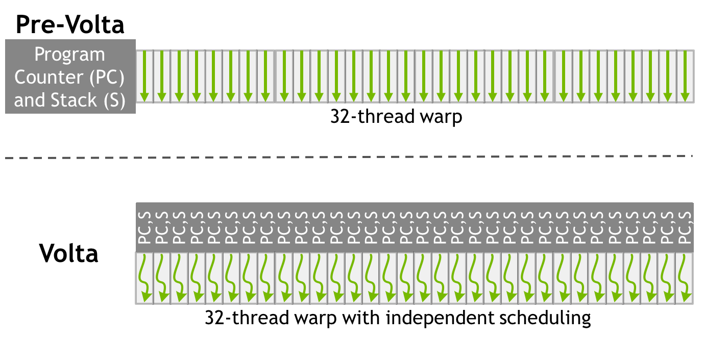
Finally, while the full details on this will have to wait until later, NVIDIA has also unveiled that they’ve made a pretty significant change to how SIMT works for Volta. The individual CUDA cores within a 32-thread warp now have a limited degree of autonomy; threads can now be synchronized at a fine-grain level, and while the SIMT paradigm is still alive and well, it means greater overall efficiency. Importantly, individual threads can now yield, and then be rescheduled together. This also means that a limited amount of scheduling hardware is back in NV’s GPUs.
Overall, GV100 is a 3 billion dollar R&D project for NVIDIA, their largest project to date for their largest GPU to date. NV is expecting the first GV100 products to start shipping in Q3 of this year and they won’t be cheap – on the order of $18K per GPU for a DGX system – however for those customers with deep pockets and who will essentially pay NVIDIA to eat the risk of producing such a large GPU, this will be the most powerful GPU released yet.
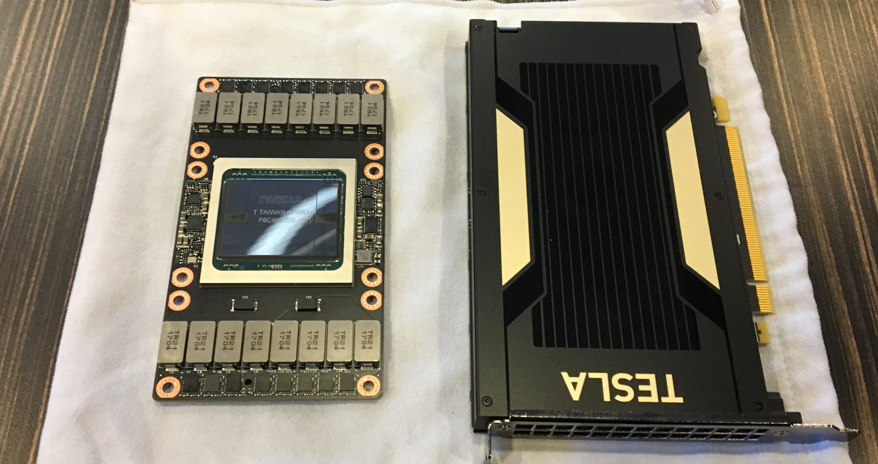
Tesla V100
The first product to use the GV100 GPU is in turn the aptly named Tesla V100. Like its P100 predecessor, this is a not-quite-fully-enabled GV100 configuration. Overall, only 80 of 84 SMs are enabled for yield reasons.
| NVIDIA Tesla Family Specification Comparison | ||||||
| Tesla V100 | Tesla P100 | Tesla K40 | Tesla M40 | |||
| Stream Processors | 5120 | 3584 | 2880 | 3072 | ||
| Core Clock | ? | 1328MHz | 745MHz | 948MHz | ||
| Boost Clock(s) | 1455MHz | 1480MHz | 810MHz, 875MHz | 1114MHz | ||
| Memory Clock | 1.75Gbps HBM2 | 1.4Gbps HBM2 | 6Gbps GDDR5 | 6Gbps GDDR5 | ||
| Memory Bus Width | 4096-bit | 4096-bit | 384-bit | 384-bit | ||
| Memory Bandwidth | 900GB/sec | 720GB/sec | 288GB/sec | 288GB/sec | ||
| VRAM | 16GB | 16GB | 12GB | 12GB | ||
| Half Precision | 30 TFLOPS | 21.2 TFLOPS | 4.29 TFLOPS | 6.8 TFLOPS | ||
| Single Precision | 15 TFLOPS | 10.6 TFLOPS | 4.29 TFLOPS | 6.8 TFLOPS | ||
| Double Precision | 7.5 TFLOPS (1/2 rate) |
5.3 TFLOPS (1/2 rate) |
1.43 TFLOPS (1/3 rate) |
213 GFLOPS (1/32 rate) |
||
| GPU | GV100 (815mm2) |
GP100 (610mm2) |
GK110B | GM200 | ||
| Transistor Count | 21B | 15.3B | 7.1B | 8B | ||
| TDP | 300W | 300W | 235W | 250W | ||
| Cooling | N/A | N/A | Active/Passive | Passive | ||
| Manufacturing Process | TSMC 12nm FFN | TSMC 16nm FinFET | TSMC 28nm | TSMC 28nm | ||
| Architecture | Volta | Pascal | Kepler | Maxwell 2 | ||
By the numbers, Tesla V100 is slated to provide 15 TFLOPS of FP32 performance, 30 TFLOPS FP16, 7.5 TFLOPS FP64, and a whopping 120 TFLOPS of dedicated Tensor operations. With a peak clockspeed of 1455MHz, this marks a 42% increase in theoretical FLOPS for the CUDA cores at all size. Whereas coming from Pascal, for Tensor operations the gains will be closer to 6-12x, depending on the operation precision.
The Tesla V100 will be paired with 16GB of HBM2. At this time no one is producing an 8-Hi HBM2 stack, so NVIDIA cannot expand their memory capacity at 4 stacks. However the memory clockspeed has improved by 25% over Tesla P100, from 1.4Gbps to 1.75Gbps.
Also like the Tesla P100, NVIDIA is using a mezzanine card. They have not shown the new connector – expect it to have more pins to account for the additional NVLinks – but the overall size is similar. NVIDIA calls this the SXM2 form factor.
In terms of power consumption, Tesla V100 will have a TDP of 300W, like its predecessor. NVIDIA notes that power efficiency of V100 is higher than P100, though it will be interesting to see just where this stands, and how often the card actually power throttles.
The first product to ship with Tesla V100 will be the NVIDIA DGX-1V, the Volta version of their DGX server. Similar to their Pascal launch, starting with DGX sales allows NVIDIA to sell 8 GPUs in one go, and for a premium at that. A DGX-1V will set you back a cool $149,000. The payoff? It ships in Q3, whereas OEM P100 designs won’t be available until Q4.
Finally, along with the mezzanine version, NVIDIA has also announced two PCIe versions of the V100. The first is a full size 250W card, analogous to the PCIe Tesla P100. The second is a smaller full height half length PCIe card, which for now is being dubbed the “Tesla V100 for Hyperscale Inference”. This is a 150W card, and is specifically meant for dense configurations in datacenter inference servers. The specifications have not been published yet, but given that it has half the TDP of the mezzanine card, it’s a safe bet that it’s clocked lower and features more disabled SMs than the full fat version.


179 Comments
View All Comments
Meteor2 - Thursday, May 11, 2017 - link
You must be on some strong chemicals.Ryan Smith - Thursday, May 11, 2017 - link
"Lastly, when you enjoy generous sponsorship from nvidia (and NOT from amd), you are inclined to overexponate."To be clear here, this isn't a sponsored trip. AnandTech is paying its own way on this (and our other) trade show trips.
Yojimbo - Thursday, May 11, 2017 - link
There are significant changes to GV100 as compared to the GP100. They expanded the SIMT model to be able to deal with thread divergence differently and allow fine-grained locking. They enhanced the L1 cache to allow code to take advantage of the GPU with less manual tuning. They reduced instruction and cache latencies. They added dedicated INT32 cores to the SMs. The unified memory management has been enhanced and hardware acceleration for parts of the CUDA multi-process server were added.The GV100 has 40% more SMs than the GP100 but less than 40% more transistors. They both have the same amount of L2 cache and register files per SM, while GV100 has 128 KB of configurable L1 cache/shared memory per SM compared to GP100's smaller and inflexible 24KB of L1 and 64KB of shared memory. GV100 also contains two extra warp schedulers per SM and a new L0 instruction cache that's apparently faster than their old instruction buffer. Add in the independence of the INT32 cores. Then consider that the cores needed to be properly meshed together to allow the tensor cores to work properly (I don't know how they work, but I can't imagine the tensor cores are completely separate units considering the lack of extra transistors in the GV100. If they added entirely new execution units for the tensor cores without increasing the transistor count per SM that would require an even more impressive reworking of the SM.) All this with less transistors per SM for the GV100 GPU compared to the GP100. Obviously, the SMs were seriously reworked.
We haven't seen how significant the architectural changes are in terms of graphics, yet, but in terms of compute, Volta significantly ups the game for allowing easier and more extensive extraction of data parallelism in workloads and for the acceleration of deep learning.
Yojimbo - Thursday, May 11, 2017 - link
Oh, in that whole post I forgot about what's perhaps the biggest indication of massive changes between the GV100 and the GP100. The Tesla V100 is 50% more power efficient than the Tesla P100 even though the power efficiency gains from the underlying process technologies (16FF+ to 12FFN) cannot possibly approach anywhere near that number.mat9v - Thursday, May 11, 2017 - link
15Tflops / 10.6Tflops = 41.5% more performance from the same power. There is no need to account for clock changes as we are not looking for IPC.BTW, IPC generation to generation increased by 2.6% so not much, probably they put most of their work into creating Tensor Cores and optimizing transistor usage (space) for increased performance.
eddman - Friday, May 12, 2017 - link
Flops =/= performanceCiccioB - Friday, May 12, 2017 - link
Your transistor "count" is somewhat wrong.You can't say it has 40% more SM with less than 40% more transistor.
A GPU is not made only of shaders or SM. Just a part of it (though large) is occupied by what is considered the core. There's also the uncore part which has not scaled and so didn't require extra transistors.
For example memory controller is the same in GV100 e GP100. ROPs (which care not so small) are the same. So those 6 billions new transistors have to be divided almost "only " between the new ALUs and TMUs (don't know the impact on thread scheduler).
Seen what's inside a GM200 with its 8 billions transistors, this 6 billions transistors means that nvidia has added a complete new GM200 (memory and bus controllers aside) to GP100. So there are enough transistor for anything.
I too do not know if tensor flow is just a repath of old ALUs or a complete new optimized SIMD block (seen the number it can be a repath) as I do not know how difficult can be setup the path for configuring the TensorCore on request and then continue with other calculations (FP16 and INT32 that are used by the TensorCore) at next instruction.
By the way the 6 billions transistors are quite a lot of transistor to be used for computation resources and it does not imply that the SM had to be "shrink" in transistor number to accommodate the new ALUs.
Yojimbo - Friday, May 12, 2017 - link
"Your transistor "count" is somewhat wrong.You can't say it has 40% more SM with less than 40% more transistor."
Yes, I can say that. It's a verifiable fact.
"A GPU is not made only of shaders or SM. Just a part of it (though large) is occupied by what is considered the core. There's also the uncore part which has not scaled and so didn't require extra transistors."
Yes, I know that, CiccioB, but approximation is the best we can get. It's a flawed approximation, but I don't think it's a useless one. And comparing the GP100 and GV100, two chips with very similar architectures (both use HBM2, etc), aimed at the same market, one with 60 SMs and the other with 84, should result in a reasonably good approximation. Yes, one would expect the total number of transistors per SM to fall with more SMs, but the SMs take up the bulk of the transistors on the chips, and other parts of the chip have similarly been scaled up in size, such as the ROPs and texture mapping units. There could of course be big changes in the size of the NVENC and NVDEC blocks, etc, in which case we'd be a bit out of luck. Comparing GM200 to GP100 is not a good idea, btw. GM200 does not contain a significant number of 64 bit capable FP units in its SMs. Better to compare the GM200 with the GP102.
What I see is that both Maxwell and Pascal seem to both add a significant number of transistors per core over their immediate predecessors. The performance improvements in Maxwell over Kepler seemed to come via having more performance per core than Kepler at the same clock, while transistors per core rose. The performance improvements in Pascal over Maxwell seemed to come primarily from higher clock rates enabled, while transistors per core rose. GV100 seems to get its performance increase primarily by being more energy efficient than Pascal. Significantly more cores can be added and run at the same clock speed as the GP100 while maintaining the same total power draw. GV100 seems to maintain the clock speed boost from Pascal, add new flexibility and features to its SMs, but yet still maintain a similar transistors per SM count as Pascal, or possibly even walk it back slightly.
A significant number of features were added to each SM in the GV100, as noted. It's a very rough calculation and far from perfect, but I think my approximation has merit.
CiccioB - Monday, May 15, 2017 - link
Of course approximation is required while talking about this matter, but I just had the impression that you were trying to split the hair over the transistor numbers with respect to the number of added ALUs.SM are a big part of the GPU die, but they are not the whole part as I said.
If you scale only the SMs at net of memory controller, ROPs and thread manager, you'll end up with a number of added transistor that justify the addition of the new ALUs (all of them as independent ALUs) without believing that the SM transistor count has to be shrunk to accomodate them all.
I made the comparison with GM200 just to show how many things you can put in 6 billions transistors. Of course SM comparison can't be made, but in GM200 8 billions transistors you have 3000+ FP32 ALU, 384bit MC, 96 ROPs, 176TMU, that is a complete beefed up GPU.
What we see is the add of 6 billions transistors only for the core part of the GPU. Which are not few.
Yojimbo - Monday, May 15, 2017 - link
"If you scale only the SMs at net of memory controller, ROPs and thread manager, you'll end up with a number of added transistor that justify the addition of the new ALUs (all of them as independent ALUs) without believing that the SM transistor count has to be shrunk to accomodate them all."You said my claim was too strong considering the approximations that need to be made and now you've gone on to make a claim just as strong as mine. What reason do you have to believe this?