The NVIDIA Titan V Preview - Titanomachy: War of the Titans
by Ryan Smith & Nate Oh on December 20, 2017 11:30 AM ESTMeet Titan V
Having quickly covered the core architecture, let’s talk about GV100 and the Titan V itself.
Like Pascal before it, for Volta NVIDIA has decided to start big, kicking off the architecture with its flagship compute GPU design, and then letting that cascade down in the future. And NVIDIA didn’t just start big in a metaphorical sense, but in a literal sense as well. At 815mm2 GV100 is massive, even by GPU standards.
This massive GPU comes even after NVIDIA has jumped nodes to TSMC’s highly optimized 16nm FinFET descendant, the aptly named 12nm FFN(vidia) process. At 21.1 billion transistors, NVIDIA has invested all of their gains and then some back into more GPU hardware, pushing the envelope on performance like never before. This is a big part of what makes GV100 such a powerful GPU, though one can only speculate what this is doing for chip yields. Titan V is very clearly a bin for chips that don’t meet the higher requirements of the Tesla V100, and NVIDIA in turn seems to have plenty of Titan V cards available.
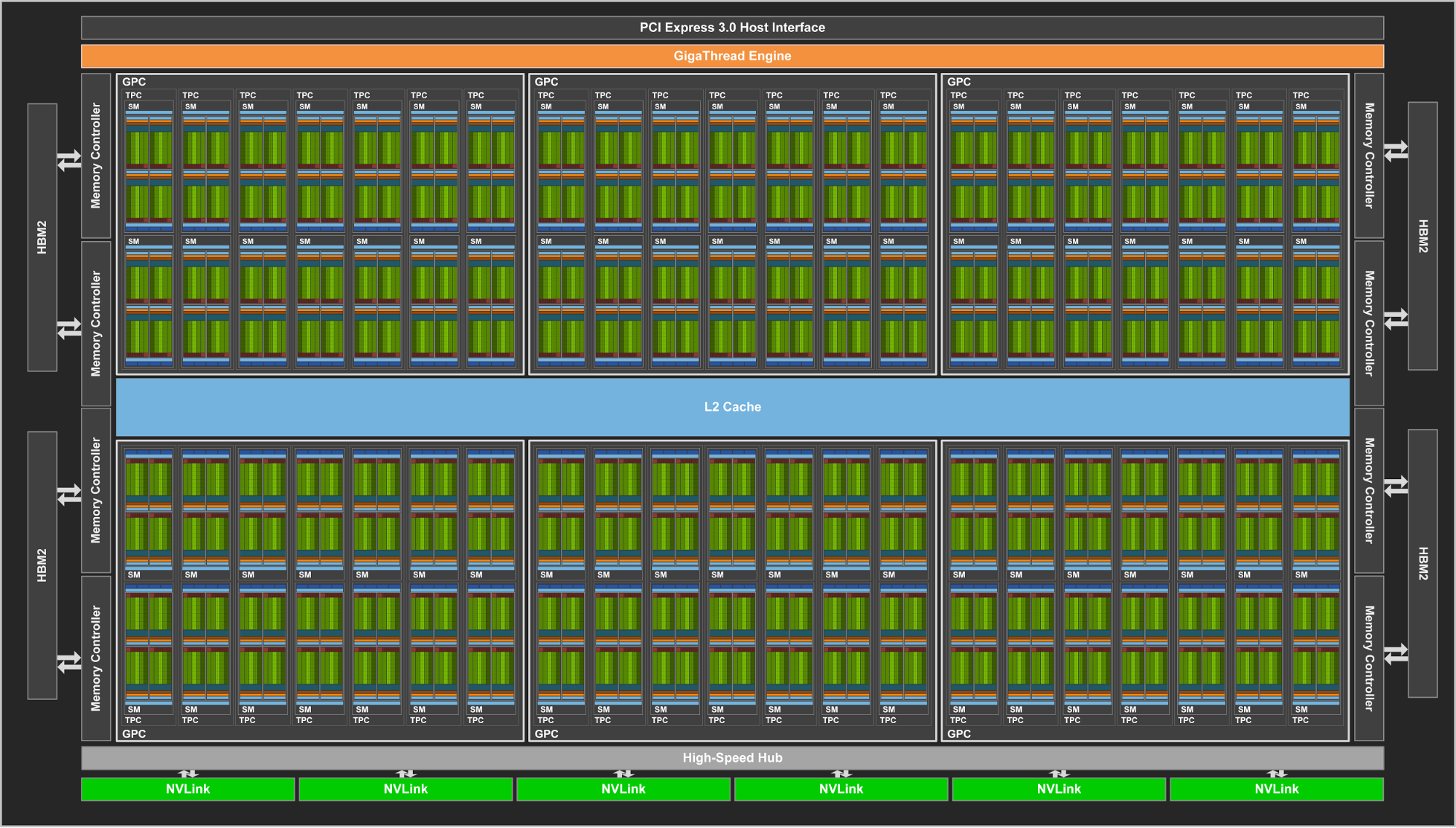
By the numbers, GV100 contains 84 SMs. Each SM is, in turn, contains 64 FP32 CUDA cores, 64 INT32 CUDA cores, 32 FP64 CUDA cores, 8 tensor cores, and a significant quantity of cache at various levels. Due to the aforementioned size of the GPU and yield management needs, no product ships with all 84 SMs enabled. Rather both Tesla V100 and Titan V ship with 80 SMs enabled, making for a total of 5120 FP32 CUDA cores and 640 tensor cores.
Like its compute-centric predecessor, GP100, GV100 retains a unique ratio of 64 CUDA cores per SM rather than the usual 128 per SM. This means the ratio of control hardware, cache, and register files to CUDA cores is much higher than on consumer parts. For a compute-centric GPU this makes a lot of sense, however after what NVIDIA did with Pascal and limiting this design to just GP100, it’s worth noting that it’s entirely possible that we’ll see an entirely different SM arrangement on future consumer Volta GPUs.
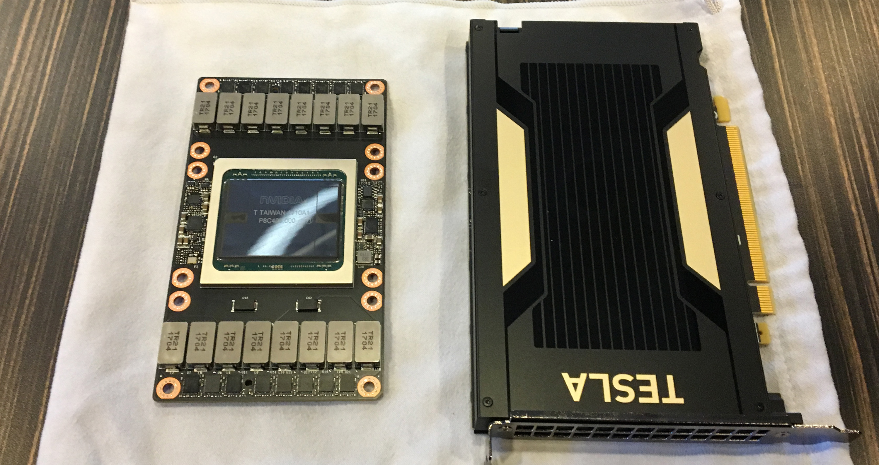
Also like GP100 before it, GV100’s memory of choice is HBM2. All GV100 packages ship with 4 stacks of the memory, however Titan V only features 3 of those 4 stacks enabled. As this is a salvage part, presumably we’re looking at GV100 packages where there was either a failure in an HBM2 stack, or in the associated memory controller on the GV100 die itself. Either way, this means that Titan V ships with 12GB of VRAM clocked at 1.7Gbps/pin, leading to a total of 653GB/sec of memory bandwidth.
Along with the workstation-suitable card design and inability to use the Tesla driver stack, the memory difference is one of the key differentiators between the Titan V and the PCIe version of the Tesla V100. Otherwise, NVIDIA has confirmed that the Titan V gets the GV100 GPU’s full, unrestricted FP64 compute, FP16 compute, and tensor core performance. To the best of our knowledge (and from what NVIDIA will comment on) it doesn’t appear that they’ve artificially disabled any of the GPU’s core features. So for most use cases, the Titan V is extremely close to the Tesla V100.
In terms of clockspeeds, the HBM2 has been clocked at 1.7GHz, while the 1455MHz boost clock actually matches the 300W SXM2 variant of the Tesla V100, though that accelerator is passively cooled. Notably, the number of tensor cores have not been touched, though the official 110 DL TFLOPS rating is lower than the 1370MHz PCIe Tesla V100, as it would appear that NVIDIA is using a clockspeed lower than their boost clock in these calculations.
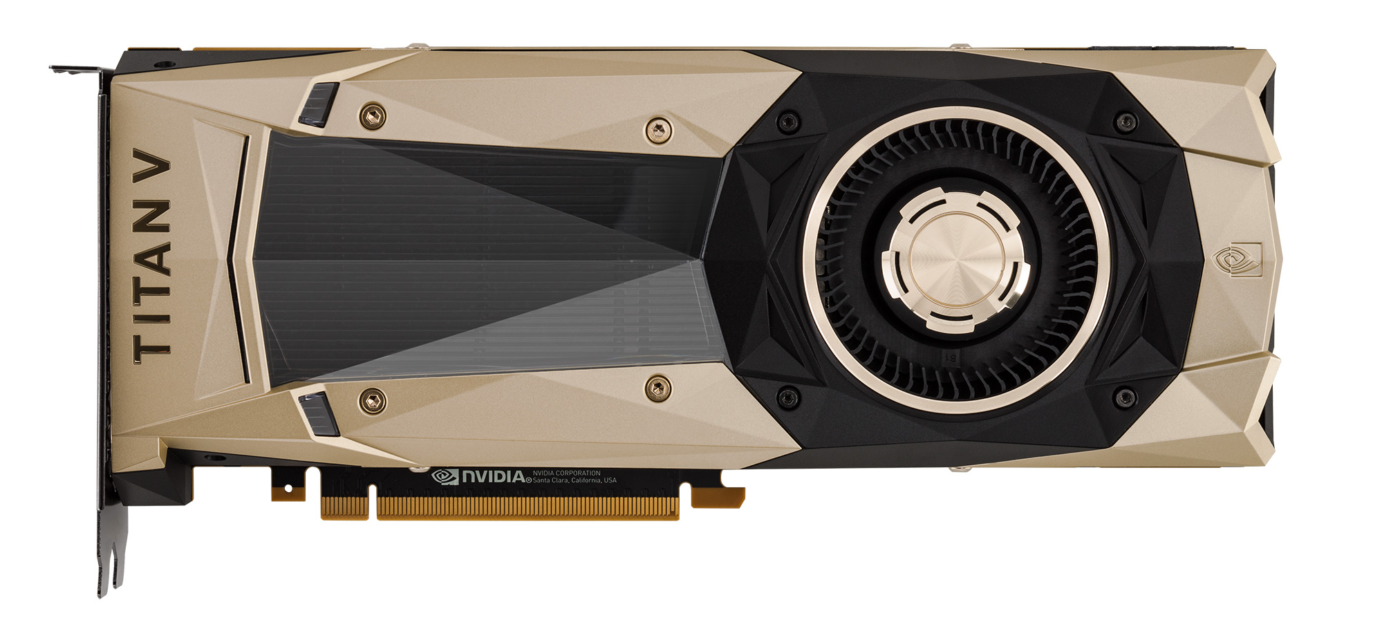
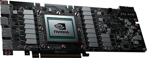
For the card itself, it features a vapor chamber cooler with copper heatsink and 16 power phases, all for the 250W TDP that has become standard with the single-GPU Titan models. Output-wise, the Titan V brings 3 DisplayPorts and 1 HDMI connector. And as for card-to-card communication, there is no SLI or NVLink support for the Titan. The PCB itself has NVLink connections on the top, but these have been intentionally blocked by the shroud to prevent their use and are disabled.
Looking at overall performance expectations then, the Titan V is clearly the fastest of the Titans. And yet outside of compute, the advantage for graphics is much smaller. Relative to the Titan Xp we’re looking at just a 14% on-paper advantage in FP32 shader throughput, and thanks to the slightly lower clockspeed an actual ROP throughput disadvantage. The real-world impact of these differences will play out differently among different programs and games, as we’ll see. But it’s an important piece of context all the same. GV100 has a lot of hardware that really only helps compute performance, and from a power standpoint that hardware is a liability. This is why NVIDIA creates differentiated consumer and compute-focused GPUs, and why GV100 isn’t quite as potent for gaming as it may seem.


A Note on Graphics Features
Before diving into our benchmarks, we also wanted to take a quick look at the graphics features of the Titan V. As this is the first Volta card with display outputs, this is our first chance to see if Volta has any new graphics capabilities. NVIDIA for their part has not been discussing Volta’s graphics features in-depth, even with the launch of Titan V, since the focus is on compute.
The flip side to this however is that everything here should still be taken with a grain of salt. Not because it’s inaccurate for Titan V, but because it’s only accurate for GV100 on the current driver stack. This is not a graphics-focused product, and that means there’s no guarantee NVIDIA has every new/upgraded feature exposed. Or for that matter, whether future consumer chips will have identical graphics features.
| NVIDIA GPU DirectX Graphics Feature Info | ||||
| Volta (Titan V) |
Pascal (Titan Xp) |
|||
| Direct3D Feature Level | 12_1 | 12_1 | ||
| Fast FP16 Shaders | No | No | ||
| Tiled Resources | Tier 3 | Tier 3 | ||
| Resource Binding | Tier 3 | Tier 3 | ||
| Conservative Rasterization | Tier 3 | Tier 2 | ||
| Resource Heap | Tier 1 | Tier 1 | ||
All of that said, what we find is that indeed, according to NVIDIA’s drivers the graphics capabilities of the Titan V are almost identical to that of the Pascal-based Titan Xp. The latter was already a fairly advanced for its time DirectX feature level 12_1 card, which is still the highest overall feature level tier within DirectX. So any differentiation is limited to the individual features. Which in this case is that the Titan V supports conservative rasterization tier 3 rather than Titan Xp’s more limited tier 2. Outside of software developers this doesn’t mean much at the moment, but it does mean that Volta is the inflection point for when developers can treat conservative rasterization tier 3 as a GPU baseline feature here in half a decade or so.
Meanwhile, as GP100 never came to a card using the GeForce driver set – the closest it got was the Quadro GP100 – this is also our first look at an NVIDIA graphics card with fast FP16 support. A lot has been made of FP16 support in recent years for pixel shaders, as the reduced precision allows for greater shader efficiency and total throughput. The Playstation 4 Pro supports FP16 shaders, as do AMD’s Vega architecture cards.
But for the Titan V, while it has fast FP16 support in hardware, as it turns out this feature hasn’t been exposed to any APIs outside of CUDA. In both Direct3D and OpenGL, FP16 is not exposed and is promoted to FP32 instead. At this point I don’t know of any reason why it needs to be this way – NVIDIA should be able to expose fast FP16 to Direct3D – but for the moment this is not the case. This may be an early driver thing, or if NVIDIA goes the same route with consumer Volta cards as they did Pascal cards, then those cards may not even support fast FP16. In which case there’s little point in enabling fast FP16 support for pixel shaders on the Titan V.
The Test
For gaming, we've opted for 4K-only for this preview, running a subset of our games. Since this is the first Volta card we are benching, we tested both DX11 and DX12 modes for Deus Ex: Mankind Divided and Total War: Warhammer on the Titan V. Load power consumption was measured on Battlefield 1 DX11 on 1440p for the sake of consistency with past results, while average clockspeeds of games were taken at 4K.
And as for our surprise entry at the end, we utilized the venerable Framebuffer Warhead tool, using the 'frost' benchmark with the 64-bit executable. SSAA was enabled in NVIDIA drivers outside the game.
For our preview of the NVIDIA Titan V, we are using NVIDIA’s 388.59 launch driver for all of our Titan cards. Meanwhile, unless explicitly running a FP64 workload, the original GTX Titan was benchmarked with full speed FP64 disabled, as is default for this card.
| CPU: | Intel Core i7-7820X @ 4.3GHz |
| Motherboard: | Gigabyte X299 AORUS Gaming 7 (BIOS version F7) |
| Power Supply: | Corsair AX860i |
| Hard Disk: | OCZ Toshiba RD400 (1TB) |
| Memory: | G.Skill TridentZ DDR4-3200 4 x 8GB (16-18-18-38) |
| Case: | NZXT Phantom 630 Windowed Edition |
| Monitor: | LG 27UD68P-B |
| Video Cards: | NVIDIA Titan V NVIDIA Titan Xp NVIDIA GeForce GTX Titan X (Maxwell) NVIDIA GeForce GTX Titan |
| Video Drivers: | NVIDIA Release 388.59 |
| OS: | Windows 10 Pro (Creators Update) |


111 Comments
View All Comments
Notmyusualid - Friday, December 22, 2017 - link
Eth, simple O/C 82MH/s.I bow before thee...
Dugom - Saturday, December 23, 2017 - link
Will you test the 388.71 ?The 388.59 doesn't support officialy the TITAN V...
Nate Oh - Saturday, December 23, 2017 - link
Yes, it does. On page 7 of 388.59 Release Notes: "New Product Support: Added support for the NVIDIA TITAN V" [1].[1] https://us.download.nvidia.com/Windows/388.59/388....
karthik.hegde - Sunday, December 24, 2017 - link
Why no one is talking about the Actual FLOPS/Peak FLOPS ? Clearly, achieving a constant 110TFLOPs that Titan has at disposal is simply not possible. What's the consistent FLOPS it can achieve before Memory Bandwidth becomes a bottleneck? When 12GB of VRAM isn't enough to hold all your data (Neural net training), then you're doing as good as previous gens.mode_13h - Wednesday, December 27, 2017 - link
That's why you use batching, sampling, and ultimately pay the big bucks for their Tesla hardware.Shaklee3 - Wednesday, December 27, 2017 - link
To the authors: what matrix size and what sample application did you use to hit 100TFLOPS on the tensor benchmark?mode_13h - Thursday, December 28, 2017 - link
You might have better luck getting a response either on Twitter or perhaps this thread:https://forum.beyond3d.com/threads/nvidia-volta-sp...
In fact, the first post on that page seems to answer your question.
linksys - Saturday, January 6, 2018 - link
nice post it is.<a href="https://www.interspire.com/forum/member.php?u=5179... Router Customer Service</a>