The NVIDIA Titan V Deep Learning Deep Dive: It's All About The Tensor Cores
by Nate Oh on July 3, 2018 10:15 AM EST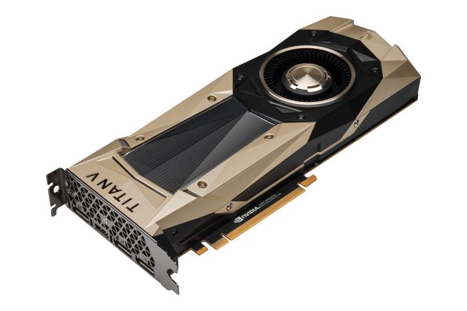
When we last discussed the NVIDIA Titan V in our preview, it was only a few weeks after its surprise launch at the 2017 Neural Information Processing Systems conference. We came away with the understanding that the Volta-based Titan V was a new breed of NVIDIA’s prosumer line of video cards, one that essentially encapsulated NVIDIA’s recent datacenter/compute achievements and how they got there. Which is to say, deep learning and neural networking has quickly become the driving force behind NVIDIA GPUs as state-of-the-art compute accelerators, now incorporating built-in hardware and software acceleration for machine learning operations. Deep learning prowess is the calling card of the Titan V and of Volta in general, and that performance is what we will be investigating today.
The most eye-catching of Volta’s new features are the new specialized processing blocks – tensor cores – but as we will see, this is very much integrated with the rest of Volta's microarchitectural improvements and surrounding software/framework support for deep learning (DL) and high performance compute (HPC). Matching up with the NVIDIA Titan V are the Titan Xp and GeForce GTX Titan X (Maxwell), with the AMD Radeon RX Vega 64 also present for some tests.
| NVIDIA GPU Specification Comparison | ||||||
| Titan V | Titan Xp | GTX Titan X (Maxwell) | GTX Titan | |||
| CUDA Cores | 5120 | 3840 | 3072 | 2688 | ||
| Tensor Cores | 640 | N/A | N/A | N/A | ||
| ROPs | 96 | 96 | 96 | 48 | ||
| Core Clock | 1200MHz | 1485MHz | 1000MHz | 837MHz | ||
| Boost Clock | 1455MHz | 1582MHz | 1075MHz | 876MHz | ||
| Memory Clock | 1.7Gbps HBM2 | 11.4Gbps GDDR5X | 7Gbps GDDR5 | 6Gbps GDDR5 | ||
| Memory Bus Width | 3072-bit | 384-bit | 384-bit | 384-bit | ||
| Memory Bandwidth | 653GB/sec | 547GB/sec | 336GB/sec | 288GB/sec | ||
| VRAM | 12GB | 12GB | 12GB | 6GB | ||
| L2 Cache | 4.5MB | 3MB | 3MB | 1.5MB | ||
| Single Precision | 13.8 TFLOPS | 12.1 TFLOPS | 6.6 TFLOPS | 4.7 TFLOPS | ||
| Double Precision | 6.9 TFLOPS (1/2 rate) |
0.38 TFLOPS (1/32 rate) |
0.2 TFLOPS (1/32 rate) |
1.5 TFLOPS (1/3 rate) |
||
| Half Precision | 27.6 TFLOPS (2x rate) |
0.19 TFLOPs (1/64 rate) |
N/A | N/A | ||
| Integer (INT8) | 55.2 TOPS (4x rate) |
48.4 TOPS (4x rate) |
26.4 TOPS (4x rate) |
N/A | ||
| Tensor Performance (Deep Learning) |
110 TFLOPS | N/A | N/A | N/A | ||
| Other Native INT Operations | INT32, DP4A, DP2A | DP4A, DP2A | N/A | N/A | ||
| GPU | GV100 (815mm2) |
GP102 (471mm2) |
GM200 (601mm2) |
GK110 (561mm2) |
||
| Transistor Count | 21.1B | 12B | 8B | 7.1B | ||
| TDP | 250W | 250W | 250W | 250W | ||
| Manufacturing Process | TSMC 12nm FFN | TSMC 16nm FinFET | TSMC 28nm | TSMC 28nm | ||
| Architecture | Volta | Pascal | Maxwell 2 | Kepler | ||
| Launch Date | 12/07/2017 | 04/07/2017 | 08/02/2016 | 02/21/13 | ||
| Price | $2999 | $1299 | $999 | $999 | ||
Circling back to NVIDIA’s compute endeavors, with Titan V, the Titan brand became closer than ever to workstation-class compute, featuring a high-end compute-centric GPU for the first time: the gargantuan 815 mm2 GV100. Complete with a workstation-class price tag of $3000, the Titan V doubled-down on high performance compute (HPC) and deep learning (DL) acceleration in hardware and software, while maintaining the fastest graphics performance around. Looking back, it’s a far cry from the original Kepler-based GeForce GTX Titan, a jack-of-all-trades video card that acted as enthusiast flagship with full double precision (FP64) compute for prosumers. Up until Titan V, NVIDIA’s Titan lineup more-or-less represented that design methodology, where a big GPU served as lynchpin for both compute and consumer lines.
| NVIDIA Tesla/Titan Family Specification Comparison | ||||||
| Tesla V100 (SXM2) |
Tesla V100 (PCIe) |
Titan V (PCIe) |
Tesla P100 (SXM2) |
|||
| CUDA Cores | 5120 | 5120 | 5120 | 3584 | ||
| Tensor Cores | 640 | 640 | 640 | N/A | ||
| Core Clock | ? | ? | 1200MHz | 1328MHz | ||
| Boost Clock | 1455MHz | 1370MHz | 1455MHz | 1480MHz | ||
| Memory Clock | 1.75Gbps HBM2 | 1.75Gbps HBM2 | 1.7Gbps HBM2 | 1.4Gbps HBM2 | ||
| Memory Bus Width | 4096-bit | 4096-bit | 3072-bit | 4096-bit | ||
| Memory Bandwidth | 900GB/sec | 900GB/sec | 653GB/sec | 720GB/sec | ||
| VRAM | 16GB 32GB |
16GB 32GB |
12GB | 16GB | ||
| ECC | Yes | Yes | No | Yes | ||
| L2 Cache | 6MB | 6MB | 4.5MB | 4MB | ||
| Half Precision | 30 TFLOPS | 28 TFLOPS | 27.6 TFLOPS | 21.2 TFLOPS | ||
| Single Precision | 15 TFLOPS | 14 TFLOPS | 13.8 TFLOPS | 10.6 TFLOPS | ||
| Double Precision | 7.5 TFLOPS | 7 TFLOPS | 6.9 TFLOPS | 5.3 TFLOPS | ||
| Tensor Performance (Deep Learning) |
120 TFLOPS | 112 TFLOPS | 110 TFLOPS | N/A | ||
| GPU | GV100 | GV100 | GV100 | GP100 | ||
| Transistor Count | 21B | 21B | 21.1B | 15.3B | ||
| TDP | 300W | 250W | 250W | 300W | ||
| Form Factor | Mezzanine (SXM2) | PCIe | PCIe | Mezzanine (SXM2) | ||
| Cooling | Passive | Passive | Active | Passive | ||
| Manufacturing Process | TSMC 12nm FFN | TSMC 12nm FFN | TSMC 12nm FFN | TSMC 16nm FinFET | ||
| Architecture | Volta | Volta | Volta | Pascal | ||
With Volta, there's little detail of anything other than GV100 existing, outside of Tegra Xavier’s Volta iGPU, which is also part of Drive PX Pegasus. So as it stands, Volta is only available to the broader public in the form of the Titan V, though depending on the definition of ‘broader public,’ the $9000 32GB Quadro GV100 released in March might fall under that category too.
Remaking of a Titan: Less Flagship, More Compute
Deep learning and compute aside, there are a few more factors involved in this iteration of the Titan brand. NVIDIA has less need to make a name for itself with the Titan line, of which the original GTX Titan did exactly that by invoking the NVIDIA’s K20Xs powering Oak Ridge National Laboratory’s Titan supercomputer, and then setting a new high in performance (and price). Nor is there any particular competitive pressure in pricing or performance – the GeForce GTX 1080 Ti has no direct competition while the Pascal-based Titan X/Xp has carved out a $1200 price bracket above the previous $1000 mark.
Meanwhile, it’s fair to assume pushing the reticle limit (815mm2) on a new process node (12nm FFN) with new microarchitecture and additional HBM2 packaging results in poor-yielding silicon, and thus fewer options for salvage parts, especially if they needed to be validated at enterprise level (i.e. Teslas and Quadros). So a more-prosumer-than-consumer Titan V part would be the best – and only – fit, given that the gaming performance isn’t at the level of $3000. Ultimately, as we’ve discussed prior, NVIDIA seeds academics, developers, and other researchers at a lower cost-of-entry to Tesla V100s, with the feedback contributing to ecosystem support of Volta. And on that note, while Titan V’s non-ECC HBM2 and GeForce driver stack are more consumer oriented, the card still directly benefits from software support with frameworks and APIs as part of NVIDIA’s overall deep learning development efforts. Other than NVLink, Titan V’s main compute functions (FP64, FP16, tensor core) are uncrippled, which makes sense as single node Titan V’s don’t quite cannibalize sales of NVIDIA’s other compute products. If that were to change with the Quadro GV100, cryptomining will ensure that prices are kept apart.

Taking a step back, the approach with Volta doesn’t mesh with NVIDIA’s previous approaches with Pascal and others. Instead of leading with a compute-centric big die design that could naturally cascade down the consumer stack as smaller GDDR5(x) designs for enthusiast graphics, they went for a gargantuan low-yielding die with good amounts of silicon area dedicated to brand-new non-graphics functions (i.e. tensor cores). We noted that tensor cores were a calculated bet, and broadly-speaking it was the usual tradeoff between lower-margin consumer graphics performance against lower-volume compute, one that NVIDIA could easily afford. The past couple years have put NVIDIA in pole position for raw consumer graphics performance and mindshare, while years of continued involvement at the forefront of GPU accelerated deep learning have put them in prime position to implement DL-specialized hardware with corresponding software support.
And as a side note, cryptomining demand has also thrown a wrench in matters, depleting much of the current generation products for extended periods of time. In turn, the consumer market hasn’t quite been saturated with current generation video cards, leaving NVIDIA in no rush to push out a new GeForce generation. Though with all the microarchitectural improvements over Pascal, I’m sure that Volta with disabled tensor cores could be levied as a very capable gaming product if necessary – the Titan V is still king of the hill – just not at the same margins as last generation. In any case, NVIDIA quarterly financials continue to cite high Pascal GeForce sales, and like all marquee silicon designers has leapfrogging design teams, the fruits of which we might just see in a few months.
Thinking Deep with GPUs
Whatever the case may be with the next generation consumer GeForce, the big picture is that both NVIDIA and AMD have publicly stated the necessity of GPU architecture bifurcation – one for HPC/ML, and one for graphics/gaming. For NVIDIA, considering that Pascal has been around for over 2 years now, Volta is conspicuously absent from recent speculation over the next GeForce generation. In looking at the Titan V today, it almost seems that NVIDIA’s divergence is imminent. Even in the case of a Volta-based GeForce launch, the implementation of consumer Volta would be a very big hint at the future direction of GPUs, gaming and compute alike. At the very least, it would be a smaller design with far fewer tensor cores – NVIDIA's RTX technology all but guarantees that at least some tensor cores will show up in consumer parts – and with a GDDR controller, at which point it raises the question how much of Volta was optimized for tensor core operations.
As our first analysis of DL performance of any GPU, we have not yet determined a standard set of benchmark tests, particularly due to Volta’s unique tensor cores and mixed precision capability. For this Titan V deep dive, we will be utilizing Baidu DeepBench, as well as tests from NVIDIA’s Caffe2 Docker image, Stanford DAWNBench implementations, and HPE Deep Learning Benchmark Suite (DLBS).
But before we dive into the numbers, this is an opportune time to provide some context, of which there is plenty: deep learning and GPUs, the Volta microarchitecture, and the current state of benchmarking DL performance.


65 Comments
View All Comments
SirPerro - Thursday, July 5, 2018 - link
The fancy girls with the macbook in starbucks are not exactly the target demographics for a deep learning desktop card. Or if they are, their laptop plays no part in that.This card is meant for professionals who can spend more than its price in google cloud training neural networks. For everyone else it makes absolutely no sense.
tipoo - Tuesday, July 3, 2018 - link
That Vega 56/64 in the iMac Pro pitched for deep learning also looks pretty underwhelming...Demiurge - Wednesday, July 4, 2018 - link
First of all, who "pitched" a iMac Pro for Deep Learning? Why would Apple put a $3k GPU in a model that is typically selling for $4-5k?Second, what model are you training on Vega that isn't sufficient with 2-4x the FP16/FP8/INT8 throughput of a 1080 Ti? How is that underwhelming?
mode_13h - Wednesday, July 4, 2018 - link
The GP102 in the 1080 Ti and Titan Xp doesn't support double-rate fp16. Just 4x int8 dot product, AFAIK, which you can't really use for training.Demiurge - Friday, July 6, 2018 - link
My point exactly since Vega does support double-rate FP16, among other things that the consumer GPU's typically don't support.As for the DP4A instruction, it is very much used in training.
INT8 datatype support is becoming more important, as is FP8 for reducing training time. Two more features Vega supports free of additional charge.
mode_13h - Friday, July 6, 2018 - link
If 8-bit int were acceptable for training, then why would anyone bother with fp16?Vega 10 doesn't have meaningful packed 8-bit support of any kind. It has only a couple such instructions that are intended for video compression. Vega 20 will change that, even adding support for packed 4-bit. But your comment seems oriented towards the current Vega.
Demiurge - Sunday, July 8, 2018 - link
Here's some reading (read the first line of the conclusion of the paper: Dettmers, 8-Bit Approximations for Parallelism in Deep Learning, ICLR 2016 https://arxiv.org/pdf/1511.04561.pdf):https://www.xilinx.com/support/documentation/white...
We shall disagree on "Vega 10 does not have meaningful packed 8-bit support". I'll let someone else argue with you, but I know what you mean. I don't agree, but I think I understand where you are coming from.
mode_13h - Monday, July 9, 2018 - link
Aww... don't pick a fight, then walk away!Here's the current Vega ISA doc. The only 8-bit packed arithmetic I see is unweighted blending and sum of absolute differences. AFAIK, this is not a useful degree of functionality for deep learning. If I'm wrong, show me.
http://developer.amd.com/wordpress/media/2013/12/V...
As for your first link, that deals with a *custom* 8-bit datatype, from what I can tell - not the int8 supported by Nvidia's DP4A or Vega 20 (from what we know).
Finally, your second link appears to deal *exclusively* with inference. Just like I said.
Nate Oh - Tuesday, July 10, 2018 - link
AMD says in the Vega whitepaper that INT8 SAD is applicable to several machine learning applications. It’s not new to Vega though. Various types of INT8 SAD dates back to earlier versions of GCN, and Kepler/Maxwell have single cycle packed INT8 SAD anyhow. But technically, according to AMD it is a useful degree of functionality.The real caveat to this is real-world DL performance has never been about raw operations per seconds, new instructions or not. This is one of the main points I wanted to convey with the article. (And to ward off any concerns, DeepBench does not fall under that because A) it uses DL kernels representative of DL applications and B) results are all in microseconds that are converted to TFLOPS using the kernel dimensions; TFLOPS is much is easier to present as a measure of performance.)
These instructions are only as good as their DL support. Even with ROCm/HIP/etc, Vega isn’t a drop-in replacement for a 1080 Ti, where you expect the hardware advantage to ‘just work’ in training. You have to port the model and retune with ROCm/MIOpen, HIP or OpenCL, etc., troubleshoot and make sure the hardware features you want to use is actually supported in MIOpen (if MIOpen support is even production-ready in your framework of choice), and the list goes on. Tuning guides for AMD architectures are not yet filled out on their ROCm documentation, and I couldn’t find out if packed INT8 xSAD is well-integrated as some DL primitive in MIOpen. MIOpen also still doesn’t support FP16 for RNNs, or training with CNNs, so no Rapid Packed Math there. Unless you implement these things yourself. I hope you know your GCN assembly.
What I’m trying to say is that for DL hardware (especially GPUs), software support and ecosystem are basically more important right now. If you’re more focused on the DL and not on the GPU side, then you’re more interested in the models and neural networking, less interested in low-level GPU tuning for a new architecture, only familiar with the CUDA ecosystem, and less willing to be a ROCm adventurer without immediate results that you need to publish or use.
So it’s true that Vega brings features to consumer GPUs that they don’t usually support, but using them for DL is not trivial. It’s easy to just say that it’ll work; I can tell you that sitting back in my chair I am super curious about Radeon SSG and DL’s perennial main memory bandwidth/size issue, but somebody has to go develop that implementation.
Which is a long way of stating, Vega doesn’t have packed 8-bit support as influential as Demiurge has claimed.
Links/References
https://radeon.com/_downloads/vega-whitepaper-11.6...
https://www.amd.com/Documents/GCN_Architecture_whi... (SAD for pixel shaders introduced)
http://rocm-documentation.readthedocs.io/en/latest...
http://rocm-documentation.readthedocs.io/en/latest...
https://www.hotchips.org/wp-content/uploads/hc_arc...
https://devtalk.nvidia.com/default/topic/966491/te...
mode_13h - Tuesday, July 10, 2018 - link
> AMD says in the Vega whitepaper that INT8 SAD is applicable to several machine learning applications."The NCU also supports a set of 8-bit integer SAD (Sum of Absolute Differences) operations. These operations are important for a wide range of video and image processing algorithms, including image classification for machine learning, motion detection, gesture recognition, stereo depth extraction, and computer vision."
Eh, I still don't think they mean deep learning. Probably, they're referring to some classical image processing techniques, or maybe preprocessing prior to feeding a CNN. Ideally, you might ask them for examples of where it's used, or maybe at least paper citations (which are conspicuously absent from that part of their whitepaper). But I know this was an ambitious article, so maybe it's something to keep in mind for your coverage of Vega 20.
> results are all in microseconds that are converted to TFLOPS using the kernel dimensions
Dude, that's messed up. At the very least, it shouldn't be TFLOPS unless you're actually using floating-point arithmetic. And if you're using a framework that optimizes your model (such as TensorRT, I think), I wouldn't report end performance as if it were actually using the unoptimized kernel.
> Tuning guides for AMD architectures are not yet filled out on their ROCm documentation, and I couldn’t find out if packed INT8 xSAD is well-integrated as some DL primitive in MIOpen.
Well, "Open" means open source, in this case. One could try and have a look. That said, it's a huge article and nobody could've reasonably expected you to do more. It'd be more digestible if broken into a couple installments, actually.
Anyway, the rough state of MIOpen is actually one of the main reasons we don't currently use AMD. I hope the situation changes by the time Vega 20 launches.
Anyhow, thanks for the comprehensive reply, not to mention the article. There are still a few parts I need to go back & read!