GlobalFoundries Gives 7 nm Capacity Update, Mulls Skipping 5 nm
by Anton Shilov on May 31, 2018 12:00 PM EST- Posted in
- Semiconductors
- GlobalFoundries
- 7nm
- 7LP
- 5nm
- 3nm
High-ranking executives of GlobalFoundries this month gave several updates concerning future plans of the contract maker of semiconductors. As it appears, in a bid to provide more tangible advantages to its customers and not to invest in short-lasting nodes, the company is mulling skipping 5 nm manufacturing technology like it did with the 10 nm fabrication process. In addition, the company admits that its only leading-edge fab may not have enough capacity for all of its customers at 7 nm, and some of its clients may need to work with other foundries to meet their demand.
7LP On Track for HVM, But Capacities Are Concern
Gary Patton, CTO of GlobalFoundries, said in an interview with EETimes that the company’s first-generation 7LP process technology (7 nm leading performance), which relies exclusively on DUV step and scan systems, is on-track for high-volume manufacturing in the second half of this year. One of the first customers to use this tech will be AMD, which briefly announced its 7LP Vega GPU for a couple of times already. Not everything is rosy with 7LP though.
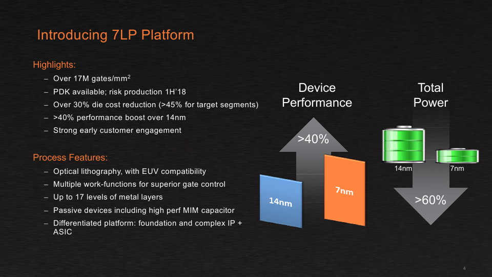
According to Mr. Patton, since the Fab 8 produces leading edge chips for all of the company’s clients, its 7LP capacity may be limited, which is why AMD may not get enough capacity. The good news is that GF’s 1st Gen 7LP is similar to TSMC’s CLN7FF (which also does not use EUV) and therefore clients with significant demand will be able to port their designs from one foundry to another with some ease. Under the wafer supply agreement signed in 2016, AMD has rights to use foundries other than GlobalFoundries in certain situations. Though whether this capacity-constrained situation actually comes to pass, and whether or not AMD and other partners of GlobalFoundries will have enough time to develop all the designs they need for both foundries should it occur, remains to be seen.
Meanwhile one thing that should be kept in mind is that GlobalFoundries is planning for three generations of 7LP processes, with two of them using EUV lithography and ASML’s Twinscan NXE steppers. As of early 2018, Fab 8 had only one EUV stepper installed with another being constructed. Meanwhile, there is a space for two more, so eventually GlobalFoundries will have four Twinscan NXE machines in Fab 8.
Capacity Expansion May Be Needed for Next Major Node
Earlier this year GlobalFoundries said that to provide its customers a tangible performance, transistor density, and power reduction boost from 7LP, it might need to move to new transistor structure. The company did not disclose any names for its next-gen node and for a reason. Apparently, GlobalFoundries is mulling whether to skip what the industry calls the 5 nm node and jump right to 3 nm. No final decision has been made and there are other concerns.
As leading edge process technologies get more complex and expensive to develop amid rising demand for chips, foundries need to boost their production capacities to remain profitable. Companies like TSMC and Samsung Foundry can land orders from large makers of consumer electronics (Apple, Samsung Electronics, etc.) that can offset development costs of nodes and equipment by ordering huge amounts of chips at premium prices. As a result, to be successful in the long term, GlobalFoundries will not only need to develop competitive process technologies, but also expand its leading edge capacities. Alternatively, GlobalFoundries is open to another process-sharing deal, like the one it signed with Samsung for their 14LPP technology.
Several years ago, GlobalFoundries already considered increasing capacity of the Fab 8 by building an additional module, but the plan was shelved back then. Instead, the company switched some of the equipment in Fab 8 to improve 14LPP supply in 2017. GlobalFoundries is still mulling whether to construct what would be Fab 8 Module 2, but a project like this might require support from the federal government, which is something that the company may not get in the USA. Meanwhile, since GlobalFoundries runs fabs not only in the U.S., but also in Germany and Singapore, another way of adding leading edge capacity would be to upgrade one or two of the non-U.S. facilities assuming that the respective governments provide incentives to the chip maker.
At present it is too early to make any predictions regarding GlobalFoundries’ plans for 5 nm or 3 nm fabrication technologies because they are years away. Meanwhile, if GlobalFoundries is seriously thinking about expanding its leading edge capacities for its next major node, it may have to make its decision rather sooner than later.
Related Reading:
- Change of Strategy: A New GlobalFoundries CEO in Dr. Thomas Caulfield
- The Future of Silicon: An Exclusive Interview with Dr. Gary Patton, CTO of GlobalFoundries
- GlobalFoundries Details 7 nm Plans: Three Generations, 700 mm², HVM in 2018
- GlobalFoundries Updates Roadmap: 7 nm in 2H 2018, EUV Sooner Than Later?
- GlobalFoundries to Expand Capacities, Build a Fab in China
- AMD Amends GlobalFoundries Wafer Supply Agreement Through 2020, Gaining New Flexibility & New Costs


19 Comments
View All Comments
FullmetalTitan - Saturday, June 2, 2018 - link
The industry consensus seems to be that 7nm will be a long-lived stable node the way 14nm has been. 5nm will be a stepping stone to 3nm, incorporating loads of new design elements. I expect there will be some pretty gnarly growing pains when everyone begins 5nm testing.AJ_NEWMAN - Thursday, May 31, 2018 - link
Could this be more about EUV with a NA change of 0.33 -> 0.55 could enable a 2 node shrink?https://electroiq.com/euvl-focus/2018/03/12/2018-s...
AJ
FullmetalTitan - Saturday, June 2, 2018 - link
High NA EUV is years away yet, but it's good news that they demonstrated a pellicle with only 2% attenuation finally, that number had been at 10% for a while (and 250W power source was under the industry expectation by about 50%).zodiacfml - Friday, June 1, 2018 - link
They should. The crypto market (ASICs, GPUs) alone is large enough to justify the investment. Add AI and gaming markets, it becomes a no brainer.As already mentioned, they should decide soon as Samsung and TSMC are aggressive.
iwod - Friday, June 1, 2018 - link
The problem is no one knows how long these will last. AI winter, GPU Crypto etc. Fabs take lots of money and time. ( Although TSMC manage to built one within 6 months )I do think it is a they should invest more and attract customer like Qualcomm Broadcom to leading node. If they are not in it for a fight then go back to do secondary node like UMC.
FullmetalTitan - Saturday, June 2, 2018 - link
Building a FAB is easy compared to the next part. Tool in and ramp are like 100x harder and always take longer because of quality verification needs.The biggest issue in leading node design is cost of development, especially in relation to troubleshooting and reticle revisions. That is only going to get worse as EUV is introduced to designs, because reticle costs are an order of magnitude more when dealing with an EUV reticle than a KrF/ArF system, and yields for EUV masks from the gold standard mask makers are still much much lower than for a DUV reticle
boeush - Friday, June 1, 2018 - link
"over 17 million gates per square mm" - well, a square mm is 1,000,000 nm x 1,000,000 nm, so that makes for ~5882 square nm per gate, or in other words if a gate is visualized as a square, it would be ~76 nm on each side. Granted, that includes spacing between gates - but is still about 10x the claimed minimum feature size (~7 nm).Of course, a logic gate these days is still canonically composed from several transistors. One thing to consider in terms of future tech R&D might be to search for simpler, smaller, alternative nano-scale structures and/or materials that can behave like various logic gates but are not built from transistors... Then we might yet squeeze another factor of 100 or more in performance from greater planar gate density, before we hit the ultimate atomic/molecular/quantum wall and have to start evolving our curcuit designs into the 3rd dimension (with all the attendant manufacturing and cooling challenges...)
FullmetalTitan - Saturday, June 2, 2018 - link
That was poor language choice. They 100% meant transistor density, not logic block density. Dense regions like SRAM are going to be far beyond that number, and there is enough dark silicon that the overall average comes down to that final number.The scaling issue for transistors in the FinFET era is that they still need multiple layers to create the proper work function (doped silicon, oxide dielectric, interfacial layer, several gate metal layers, active gate polysilicon, another metal layer, and W plug to connect to MOL interconnects). These films are already controlled at the single-digit nm (and sometimes single-digit A) scale. The move to nanowires, or gate all around, is an attempt to increase effective gate length/size for effective transistor switching control, without making the gate PHYSICALLY larger. Most work in node "shrinks" is just geometry tweaks to make the gate more efficient, stress tweaks to make gates faster/slower, etc.
levizx - Friday, June 8, 2018 - link
That's nonsense.1. 7nm is not the claimed Minimum Feature Size, rather process name used to refer to Gate Length up until 28nm.
2. you essentially calculated MMP x CPP, that was NEVER EVER the feature size. Even before FinFET, it's been 3x ~4x the feature size for years - at 65nm it was ~220nm, at 0.13um it was ~ 0.35um.