Samsung Ships First Commercial Embedded MRAM (eMRAM) Product
by Anton Shilov on March 6, 2019 4:00 PM EST
Samsung today announced that it has started mass production of its first commercial embedded Magnetic Random Access Memory (eMRAM). Made using its 28FDS (28nm FD-SOI) process technology, the eMRAM module promises to offer higher performance and endurance when compared to eFlash. Furthermore it can be integrated into existing chips, according to the manufacturer.
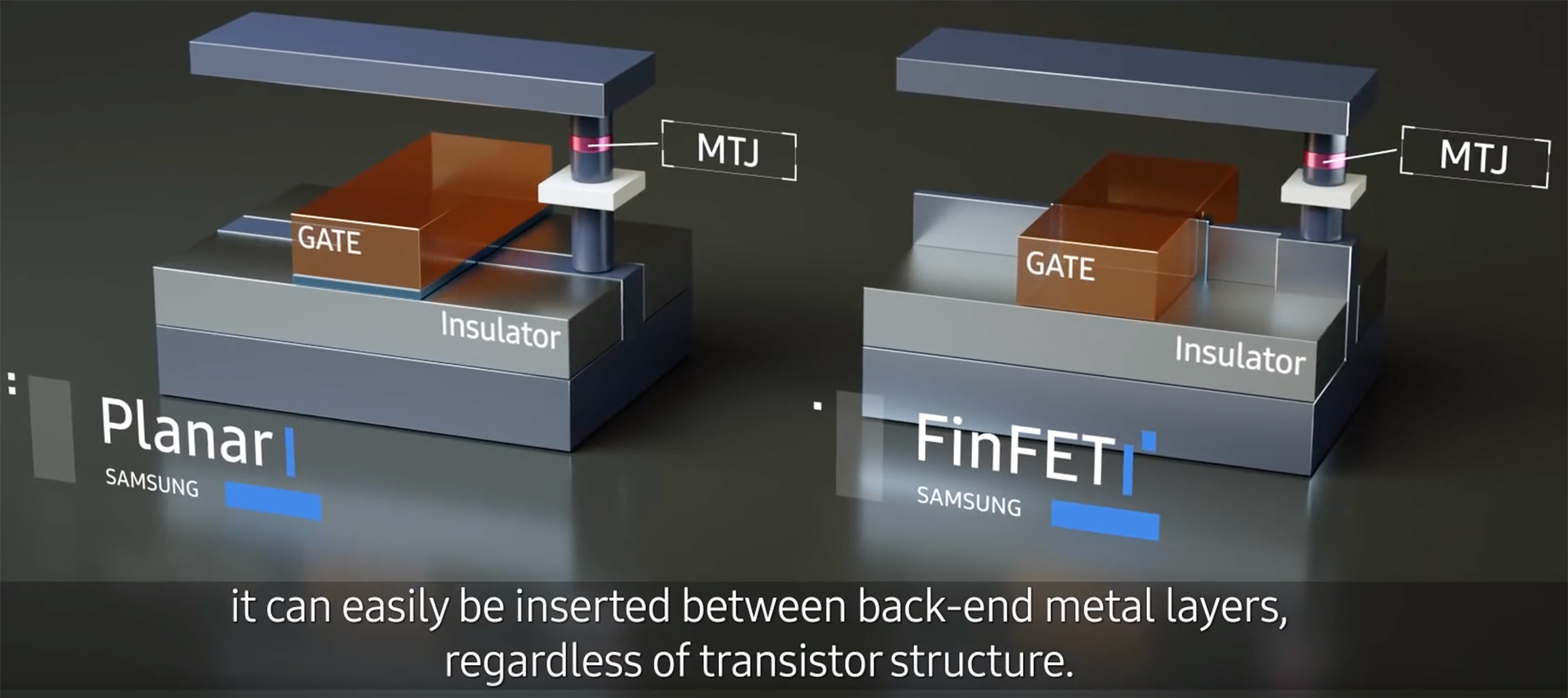
Magneto resistive RAM uses a resistance-based method that determines what data is stored in a cell, which in turn is based on reading the orientation of two ferromagnetic films separated by a thin barrier. Samsung calls this process Magnetic Tunnel Junction, or MTJ.
MRAM is one of the highest-performing and most durable non-volatile memory technologies currently exists. Because its eMRAM does not require an erase cycle before writing data, it is 1,000 times faster than eFlash, Samsung says. It also uses lower voltages when compared to eFlash, and therefore consumes around 1/400th the energy during writing process, according to the maker.
On the flip side, however, MRAM’s density and capacity both fall far short of 3D XPoint, DRAM, and NAND flash, which greatly reduces its addressable markets. Samsung is not formally disclosing the capacity of its new eMRAM module; the company is only saying that it yet has to tape out a 1 Gb eMRAM chip in 2019, which strongly suggests that the current offering has a lower capacity.
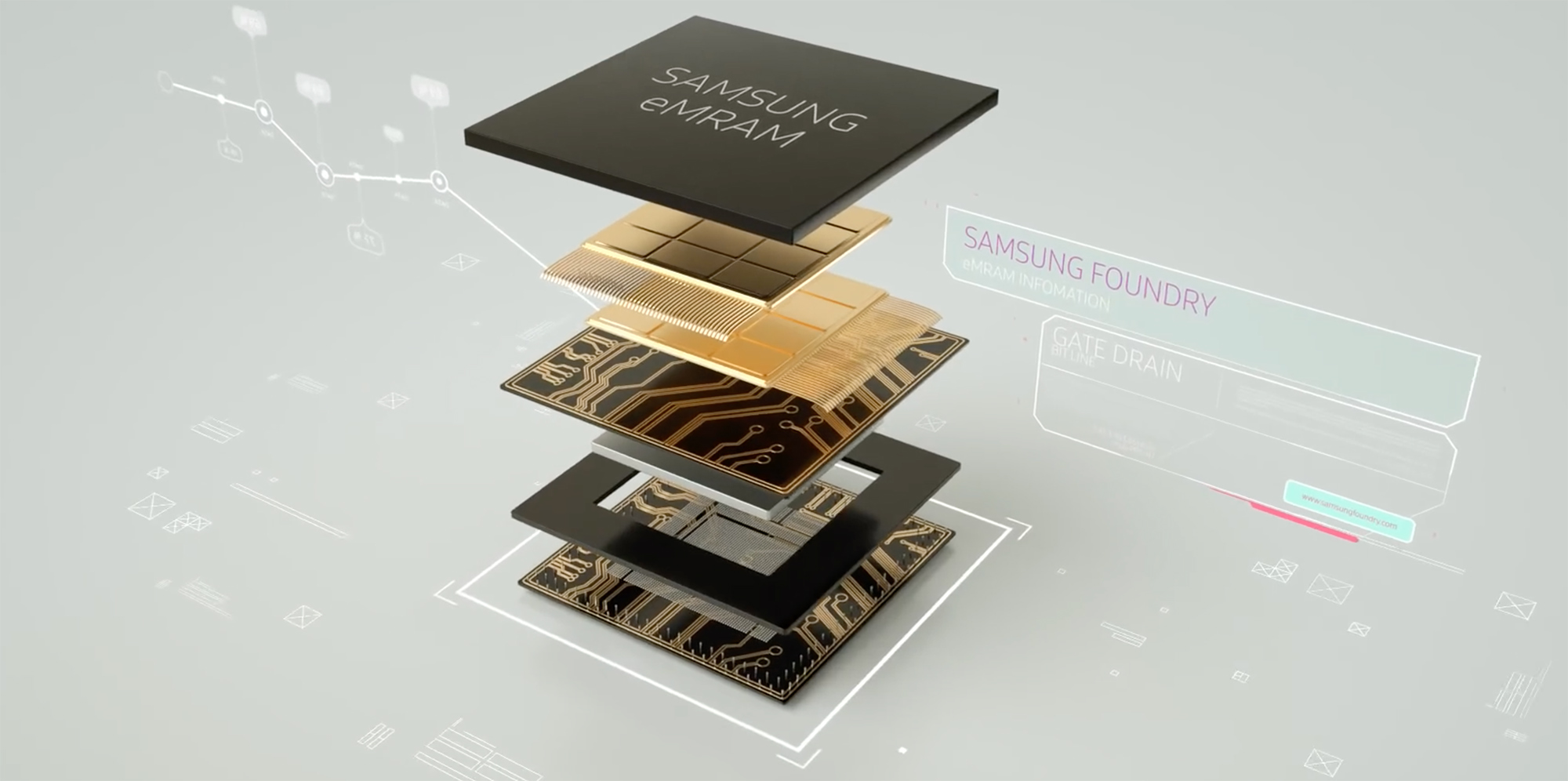
Made using Samsung’s 28FDS process technology, Samsung's eMRAM module can be integrated in the back-end of a chip's manufacturing process by adding three additional masks. As a result, the module does not necessarily depend on what front-end manufacturing technology is used, allowing it to be inserted into chips produced using bulk, FinFET, or FD-SOI fabrication processes.
Given its limited capacity, Samsung says that the module is primarilly aimed for use in microcontrollers, chips for IoT, and AI (neural network, machine learning, etc.) applications.
Meanwhile, Samsung says that it will keep expanding its embedded non-volatile memory offerings going forward. Among the upcoming options is its 1 Gb eMRAM test chip, whose tape-out is scheduled for later this year. Farther down the line still, Samsung is also planning to make eMRAM using its 18FDS process, as well as more advanced FinFET-based nodes.
Related Reading:
- IBM And Everspin Announce 19TB NVMe SSD With MRAM Write Cache
- Seagate Demos New SSD Features And Prototypes At FMS
- Everspin Announces New MRAM Products And Partnerships
- MRAM Developer Day, GlobalFoundries Keynote Live Blog
Source: Samsung


25 Comments
View All Comments
Yojimbo - Wednesday, March 6, 2019 - link
If its density and capacity is lower than that of DRAM then I don't think they are considering this as a replacement for NAND flash.danielfranklin - Thursday, March 7, 2019 - link
This isnt even for consumer devices. Its likely to have the write cycles closer to DRAM than anything you are talking about and no one is talking about replacing NAND with this, not now or in 50 years.Read FLGT's explanation above where this is going to replace situations where EEPROM & NOR currently works better than NAND.
PeachNCream - Thursday, March 7, 2019 - link
*taps the outside of your bubble* 50 years more for NAND before we talk about replacing it? I might agree if we're talking about embedded systems or ICs, but as primary storage, it's a dead man walking already from an endurance perspective. 3D QLC is rated for at most, about 1K program-erase cycles and the powered off data retention numbers aren't exactly encouraging either. Going 3D has helped a lot because we can get density by stacking layers so it somewhat mitigates the problem of smaller nodes robbing durability, but we are very much looking at the end of the road for consumer and enterprise storage.FullmetalTitan - Thursday, March 7, 2019 - link
This is very clearly being sold as a replacement for embedded memory ON CHIP, not as bulk storage. You are so eager to be a contrarian on every article that you end up looking like an idiotsaratoga4 - Thursday, March 7, 2019 - link
>*taps the outside of your bubble* 50 years more for NAND before we talk about replacing it?Nothing in the post you are replying to says anything about NAND lasting for 50 years.
PeachNCream - Friday, March 8, 2019 - link
For your ease of reference "... talking about replacing NAND with this, not now or in 50 years..."jospoortvliet - Thursday, March 7, 2019 - link
In their video they claim it has 'better endurance' without specifying how much.https://www.youtube.com/watch?v=EB14K8Gq5-w
MFinn3333 - Thursday, March 7, 2019 - link
It's most likely going to replace the DRAM in the SSD's so they can survive a power loss better or AI chips so they can keep up with what it is doing algorithm wise.It's endurance span is 10^10 writes, 10 retention @ 85°C.
PeachNCream - Friday, March 8, 2019 - link
Thanks for the numbers. The endurance and retention both look good and if it ends up as a DRAM cache replacement, that'll be sufficient to carry it there. May I ask where you found that information as I haven't had much luck scaring up anything solid.MFinn3333 - Friday, March 8, 2019 - link
I own stock in the company called 'Everspin' and that is what they are getting on their STT-MRAM products and I got it from their prospectus (voting information).