TSMC: 3nm EUV Development Progress Going Well, Early Customers Engaged
by Anton Shilov on July 23, 2019 3:00 PM EST- Posted in
- Semiconductors
- EUV
- TSMC
- 3nm
Development of new fabrication technologies never stops at leading-edge companies such as TSMC. Therefore, it is not surprising to hear the annoucement that development of TSMC’s 3nm node is well underway, something the company publicly confirmed last week. As it appears, the manufacturing technology is out of its pathfinding mode and TSMC has already started engaging with early customers.
“On N3, the technology development progress is going well, and we are already engaging with the early customers on the technology definition,” said C.C. Wei, CEO and co-chairman of TSMC, in a conference call with investors and financial analysts. “We expect our 3-nanometer technology to further extend our leadership position well into the future.”
Since its N3 technology is in its early stages of development, TSMC doesn't currently talk about the specific characteristics of the process nor its advantages over N5. TSMC said that it had evaluated all possible transistor structure options for 3nm and came out with ‘a very good solution’ for its clients. The specification is under development and the company is confident it would meet requirements of its leading partnering customer.
One of TSMC’s arch-rivals, Samsung Foundry, plans to use nanosheet-based Gate-All-Around MBCFET transistors for its own 3nm (3GAAE) process technology. Since TSMC will have to be competitive with its rival, we expect the company to also advance its 3nm node significantly in comparison to its 5nm node. In fact, TSMC confirms that N3 is a brand-new process technology, not an improvement or iteration of N5.
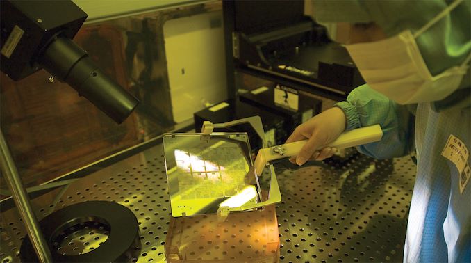
Meanwhile, it is safe to say that that TSMC’s 3 nm node will use both deep ultraviolet (DUV) and extreme ultraviolet (EUV) lithography equipment. Since TSMC’s N5 uses up to 14 EUV layers, it is likely that N3 will go even higher in the amount of layers employed. The world’s largest contract maker of semiconductors also seems to be quite happy with its EUV progress and considers the technology important for its future.
Related Reading:
- Samsung Announces 3nm GAA MBCFET PDK, Version 0.1
- TSMC’s 5nm EUV Making Progress: PDK, DRM, EDA Tools, 3rd Party IP Ready
- TSMC: First 7nm EUV Chips Taped Out, 5nm Risk Production in Q2 2019
- TSMC Details 5 nm Process Tech: Aggressive Scaling, But Thin Power and Performance Gains
- TSMC Starts to Build Fab 18: 5 nm, Volume Production in Early 2020
Source: TSMC


75 Comments
View All Comments
Wilco1 - Tuesday, July 23, 2019 - link
It's not true that transistors are frozen, transistor density is increasing rapidly each generation (eg. TSMC 7nm to 5nm is ~1.8x, and 5nm to 3nm is ~1.3x). Here is a good article detailing existing and future processes. As you can see, everything is scaling well, CPP, M2P, tracks and actual transistor density.https://semiwiki.com/semiconductor-manufacturers/i...
In any case the "nm" has had no meaning for at least 10 years and with FinFET it makes no sense at all - but all that matters is that smaller nm means higher density.
Wilco1 - Tuesday, July 23, 2019 - link
Btw a single transistor is effectively 2*CPP by track height/2, so for 7nm that would be 114nm by 120nm. So there is plenty of scope for further scaling.rahvin - Tuesday, July 23, 2019 - link
I never said transistor density isn't increasing, only that the transistor "gap" is pretty much frozen and unable to shrink further due to quantum effects.Manufacturers worked around this quantum restriction by building 3D transistors that allowed a wider gap on top of smaller traces. FinFET and other 3D transistor technology allows the wider gap to sit on smaller trace which allows transistor density to continue to increase.
saratoga4 - Tuesday, July 23, 2019 - link
>I never said transistor density isn't increasing, only that the transistor "gap" is pretty much frozen and unable to shrink further due to quantum effectsYou didn't actually say that, but if you had you would still have been incorrect.
Wilco1 - Tuesday, July 23, 2019 - link
I have no idea what exactly you mean with "gap", but certainly the gaps between transistors and individual fins are still shrinking. The fins have become thinner and taller as well with each generation. There isn't anything at all that is frozen and unable to scale further. Everything scales.Smell This - Wednesday, July 24, 2019 - link
If I recall, Kaby 14nm (++?) scaled "backwards" ~~ and it is likely that 'short-cell' transistor libraries pooched Chipzillah's 10nm . . .
Wilco1 - Wednesday, July 24, 2019 - link
Yes Intel's ++ processes typically have worse density unlike the rest of the industry.buxe2quec - Wednesday, July 24, 2019 - link
So what is that value referring to? any link explaining maybe graphically?Smell This - Thursday, July 25, 2019 - link
See if this works for you ...https://fuse.wikichip.org/news/2004/iedm-2018-inte...
name99 - Wednesday, July 24, 2019 - link
No you will not ("have gates made up of about <50 atoms soon"). Not just because of the usual whining that feature size is "marketing", but because transistors are 3D objects.Even if the smallest feature of your transistor (eg the width of a fin, which BTW is 7nm for 7nm...) is "process marketing size", the fin still has a height and a length, which boils down to incorporating a whole lot of atoms! And which shows that measuring these things in "atom widths" is meaningless; measure them in terms of something that actually matters.
If you manufacture artificial materials, like the materials used for QCLs, you lay down a one to a few atoms thick layer of atoms of type A, then another of type B, then C, then repeat 20 to 100 times. This can be done! And it works! Yes, the individual structures are one to a few atoms thick --- but they are also mesoscopically wide (ie width is microns to millimeters) so MANY MANY more than just a few atoms are involved, even when you ask about the behavior of just one layer.