Samsung Unveils 6th Generation V-NAND Memory with Up to 136 Layers
by Anton Shilov on August 6, 2019 3:30 PM EST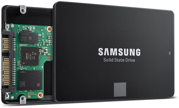
Samsung on Tuesday introduced its sixth-generation V-NAND memory, which in a bid to further improve capacity and density, features over 100 active layers. To make V-NAND with over 100 layers viable from performance point of view, the company had to use new circuit design technology. The new memory features 10% lower latencies and consumes 15% lower amount of power when compared to Samsung's previous-generation V-NAND.
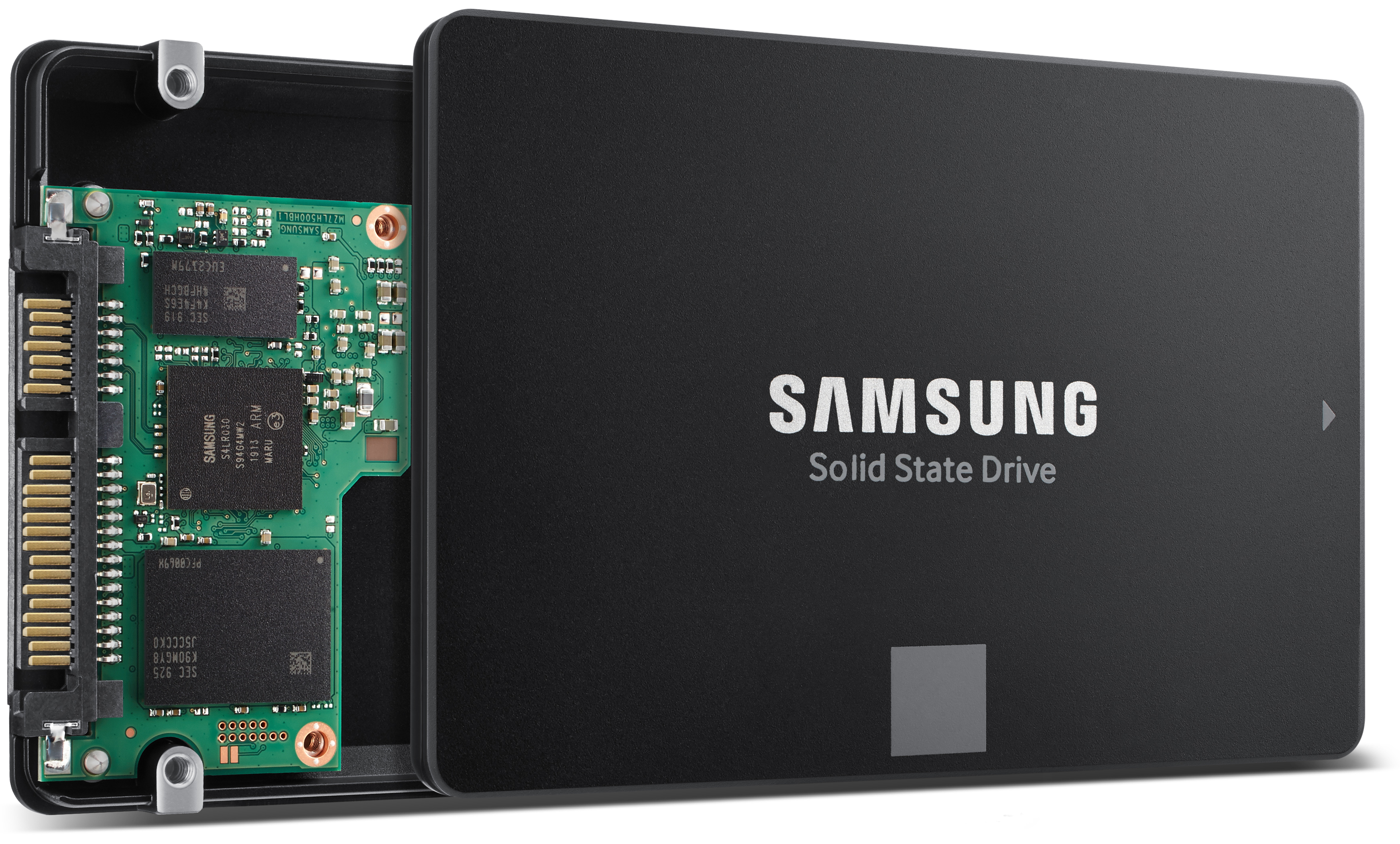
Samsung’s 6th Generation V-NAND features up to 136 layers as well as charge trap flash (CTF) cells. The new memory uses one stack and does not use technologies like string stacking to build over 100 layers. In order to ensure minimal errors and low latencies, Samsung had to use a new speed-optimized circuit design. The latter enables the new 3D TLC 256 Gb chips to offer below 450 microseconds (μs) latency for write operations and below 45 μs for read operations, which is 10% faster when compared to 5th Generation V-NAND, according to Samsung. Meanwhile, the latest V-NAND also features lower power consumption than its predecessors.
It is noteworthy that the new 256 Gb 136-layer V-NAND devices use 670 million holes, down from 930 million holes with the previous generation, which means that the new chips need fewer process steps and are easier to manufacture. What is important is that Samsung plans to use its 136-layer architecture with speed-optimized circuit design to build V-NAND devices with over 300 layers by mounting three of the current stacks on top of each other (thus tripling a chip’s capacity).
Initially, Samsung will offer 256 Gb 3D TLC 136-layer V-NAND devices that will first be used for Samsung’s 250 GB SSDs. Later this year Samsung intends to release 512 Gb 136-layer V-NAND devices that will be used for other drives as well as eUFS storage solutions.
Speaking of the 256 GB 6th Gen V-NAND SSD, it is important to point out that it uses Samsung’s new controller marked as the S4LR030/S94G4MW2.
Related Reading:
- Samsung Shares SSD Roadmap for QLC NAND And 96-layer 3D NAND
- Samsung's New 512 GB UFS 3.0 Chip for Galaxy Fold, Now in Mass Production
- Samsung Starts Production of 1 TB eUFS 2.1 Storage for Smartphones
- The Samsung 970 EVO Plus (250GB, 1TB) NVMe SSD Review: 96-Layer 3D NAND
Source: Samsung


41 Comments
View All Comments
tooto - Sunday, January 12, 2020 - link
It's 128-layer V-NAND, not 136-layer one. Data from Samsung Newsroom supports the assumption that 5th gen. features 92 layers and 6th gen. features 128 layers.Also, “an electrically conductive mold stack comprised of 136 layers” doesn't necessarily mean 'an 136-layer CTF structure'
########## ########## ########## ########## ########## ##########
9x:1xx=6.7:9.3 ~0.72 // 92:128 ~0.72 // 92:136 ~0.68 // 96:128 ~0.75 // 96:136 ~0.71