Hot Chips 31 Analysis: In-Memory Processing by UPMEM
by Dr. Ian Cutress on August 19, 2019 3:15 PM EST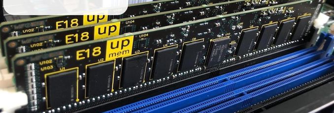
One of the key critical future elements about this world of compute is moving data about. Moving data requires power, to the point where calling data from memory can consume more power than actually doing ‘compute’ work on it. This is why we have caches, but even these require extensive management built in to the CPU. For simple operations, like bit-shifts or AND operations, the goal is to move the ability to do that compute onto the main DRAM itself, so it doesn’t have to shuttle back and forth. This year at Hot Chips, UPMEM is one of the first companies to showcase their new technology.
For anyone that has done any form of general purpose compute, pushing a bunch of inputs through an algorithm to get a result, and for those that have written the code, there are typically two high-level mental stages to conquer: first is getting it to work, and second is optimizing it. The algorithm needs to produce the correct result, and the faster the better – a slow correct result often isn’t useful, and a fast incorrect result is useless. If it can be done in less power, than that also decreases overhead.
The idea behind In-Memory Processing, or ‘Processing In-Memory’, is that a number of those simple integer or floating point operations should be done while the memory is still in DRAM – no need to cart it over to the CPU, do the operation, and then send it back. If the data can stay there and be updated, this saves time and power without affecting the result. Alternatively, perhaps compute on the CPU can be reduced if results are sent back out to main memory and a final XOR is applied to the data in memory. That frees up the main CPU core to do other compute related things, or reduces the effective memory bandwidth should it be a limiting factor.
What UPMEM has done is develop a data processing unit (DPU) that is built into the DRAM chip itself, on the DRAM process node. Each DPU has access to 64 MB of DRAM, and has the equivalent of 1 GB/s bandwidth to that memory. The DPU is built on a clean 32-bit ISA with a raft of optimizations, such 0-cycle conditional jmps, combined SHIFT+X instructions (such as SHIFT+ADD or SHIFT+SUB), basic logic instructions, shift and rotate instructions. The programming model is such that C-based libraries are in play taking care of all the common issues, and UPMEM expects for most apps for it to require a few hundred lines of code and a team of a handful of people need only take 2-4 weeks to update the software.
The big numbers that UPMEM are quoting involve better TCO, better ROI, and a potential target market of $10B. We’ll go through these in due course.
Processing In-Memory DRAM, or PIM-DRAM
(Personally I prefer the name PIM-DIMM, but oh well)
What UPMEM is proposing is a standard DDR4 RDIMM like product for which each 64 MB of memory has access to one of its DPUs. The DPU is built into the DRAM itself, using the manufacturing node that the memory is made in. For example, UPMEM is promoting that it is making a 4 Gb DDR4-2400 chip to be used in modules that embeds 8 DPUs in 512 MB, with the DPUs running at 500 MHz. UPMEM plans to put 16 of these 4 Gb chips onto a single DDR4 RDIMM module, providing an 8 GB module with 128 DPUs inside.
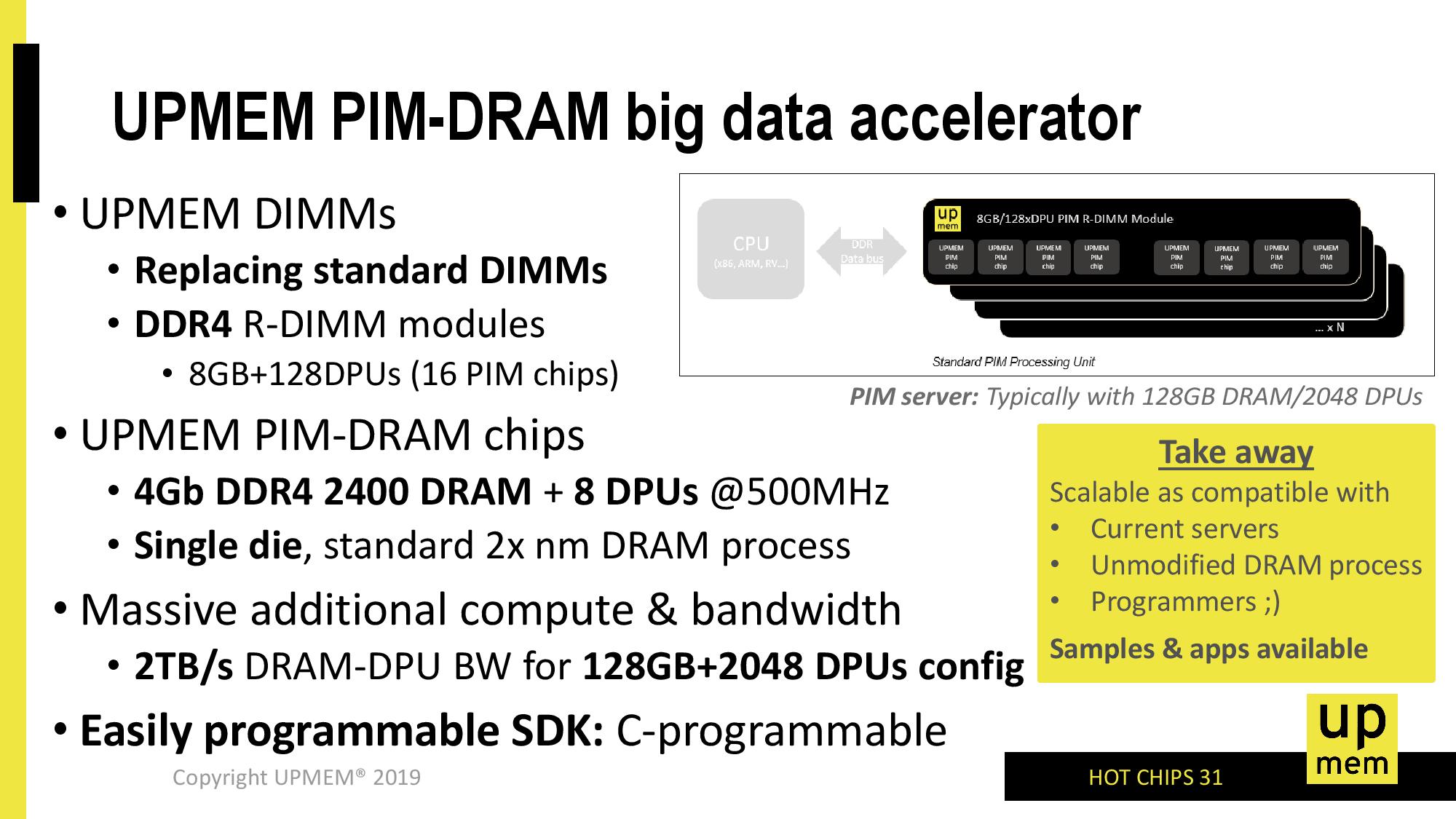
The goal is to eventually produce 128 GB modules with 2048 DPUs in total. At an effective 1 GB/s bandwidth between a DPU and its 64 MB of memory, this would imply an effective 2 TB/s bandwidth between the DPUs and memory. This is needed due to the way the DPU works, which is explained below.
The processor and technology are patented, but UPMEM has stated that they are working with a memory vendor on a 20-nm class process. Adding in the DPU cores adds a very negligible amount of die area, and can be enabled within 2-3 metal layers, as the logic is a magnitude less dense than a leading edge logic implementation. The idea is to achieve a total energy efficiency of 10x combined with scalability, compared to the leading CPU implementations.
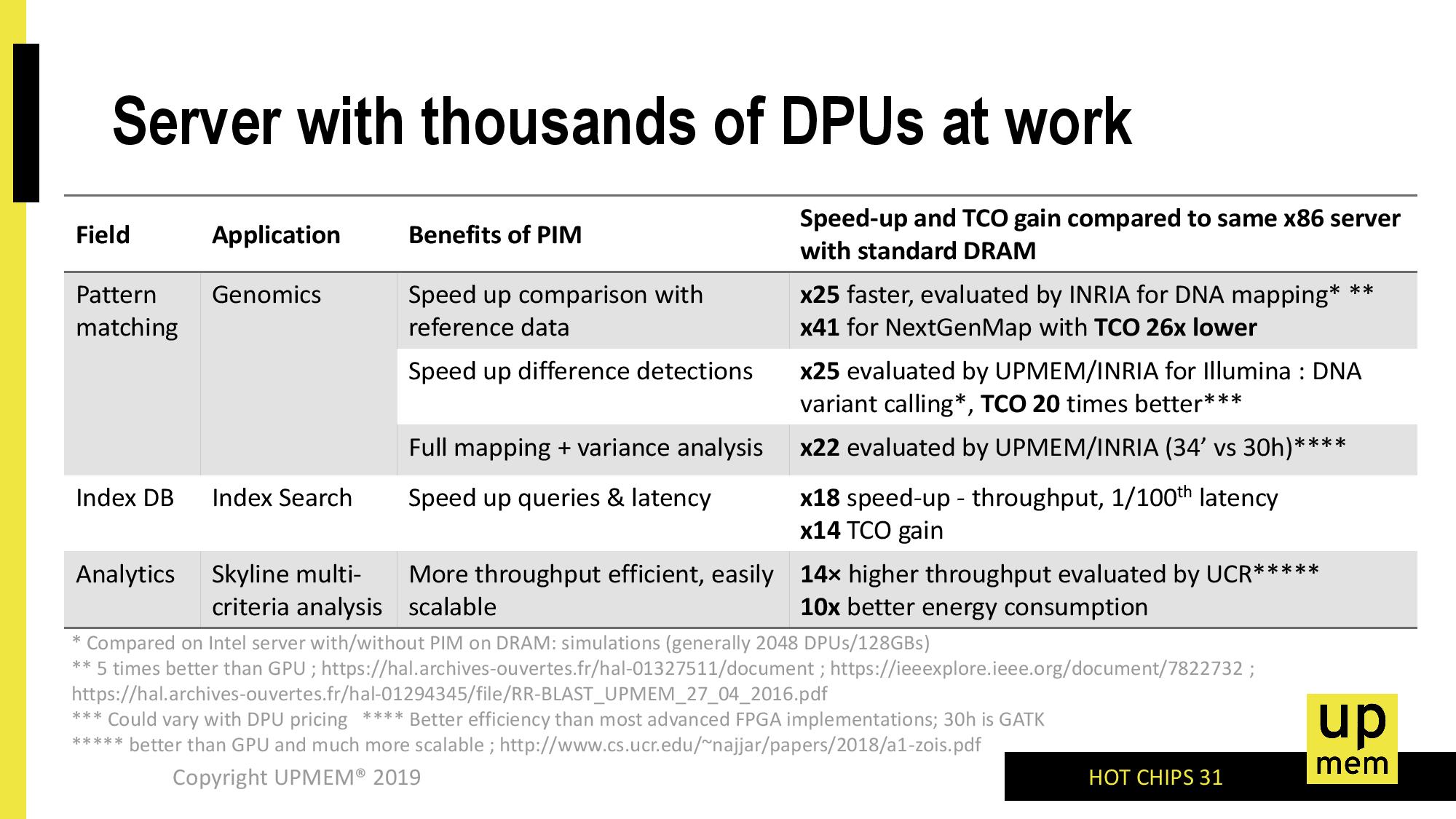
Currently UPMEM has software simulations and hardware FPGA verification simulators for customers – in fact, interested parties can emulate the UPMEM platform on an AWS f1.16x large instance. Actual PIM-DRAM module samples are shipping to high profile customers in Q3, with a plan to ramp through the next year as more parties are interested and get on-board. Citing performance examples, UPMEM has stated that they have seen speedups of 22x—25x on Genomics pattern matching, an 18x speed up in throughput for database index searching at 1/100th the latency, and an 14x TCO gain for index search applications.
On the side of cost, UPMEM hasn’t stated how much it plans to sell its technology for, but promise to be a marginal cost compared to alternative solutions. In one presentation, the company stated that their solution can replace a potential $40000 server with a $400 enhanced memory solution, noting that using PIM has knock-on effects for software licensing, datacenter space, and power consumption/efficiency.
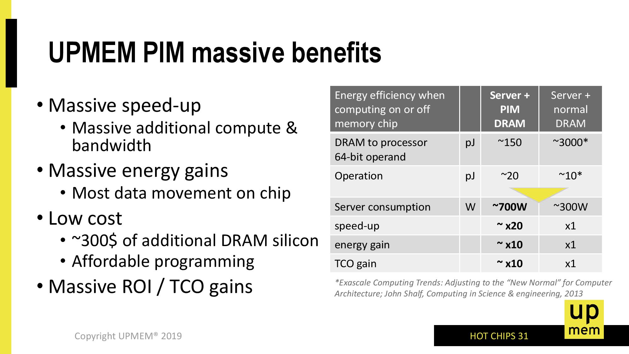
UPMEM puts some data on that power consumption. In this slide, the company compares two servers, one with PIM-DRAM and one without. In this case, a ‘DRAM to processor 64-bit operand’ recall requires 3000 pJ on a regular server, pulling the data out of DRAM and through to the caches, whereas the same operation on PIM-DRAM where it only has to move the data onto a DPU takes only 150 pJ of energy. The operation itself on the DPU actually requires 2x the power (20 pJ compared to 10 pJ), but the overall gain in power efficiency is 170 pJ vs 3010 pJ, or just under 20x.
One thing that this slide states that might be confusing is the server power consumption – the regular server is listed as only 300W, but the PIM solution is up to 700W. This is because the power-per-DRAM module would increase under UPMEM’s solution.
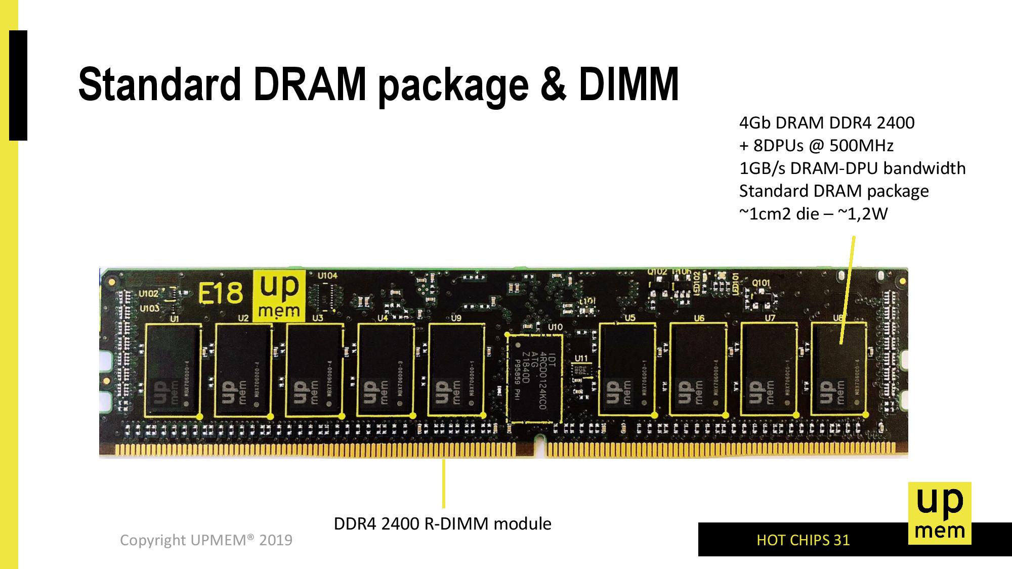
The module that UPMEM is proposing as its first product is that 8 GB DDR4-2400 module mentioned previously, with 128 DPUs each covering 64 MB of memory and running at 500 MHz. For a single 4 Gb die (there are 16 of them in an 8 GB module, 18 for RDIMM ECC), we are still at a regular 1 cm2 die size but the power required per chip is ~1.2 watts.
If we go into all 16/18 chips, we can see that each 8GB module is going to be in the 19.2-21.6 watts. That’s a lot of power for DRAM, and actually pushes up against the limit of what a DDR4 slot is often rated for. To put some perspective here, Intel’s 512 GB Optane module has an 18 W running mode for servers that can cool that much, but can run as low as 12 W. UPMEM hasn’t stated if it offers the ability for its customers to scale down the power per module by reducing the DPU frequency.
UPMEM’s goal is to replace DRAM modules in servers with PIM-DRAM modules as drop-in replacements. The company states that the DDR4 interface isn’t the best for this sort of thing, but they have worked around it. In one presentation, the company notes that at present there needs to be non-PIM-DRAM installed at a minimum for an OS.


38 Comments
View All Comments
abufrejoval - Tuesday, August 20, 2019 - link
How can it not be selfish when Facebook, Amazon and Google save data transmission capacity and compute power and use your phone and browser to mine all the personal information they sell or use?They make you the product and have you pay for it, too!
Quite the opposite of altruism in my book. And completely unethical as well.
SaberKOG91 - Tuesday, August 20, 2019 - link
The amount of power consumed by client devices and telecoms far far far exceeds data center power consumption. If you can optimize at the client level, you can save way more energy than anything you can do in the datacenter. This is why we are seeing more and more special accelerators in consumer electronics when those same accelerators aren't as prevalent in the datacenter. That's an industry trend as a whole and has nothing to do with FB, Google, or Amazon specifically.And for crying out loud, you don't get to complain about what they do with your data when you aren't paying for their services and still choose to use them. There's no such thing as a free lunch. There are plenty of alternative services to anything they offer that protect your privacy and give you more control over your data. It will cost more and will be less convenient, but if you care that much, surely you'll pay the cost?
abufrejoval - Tuesday, August 27, 2019 - link
Sure, this is an industry trend as a whole, but yes it has everything to do with FB, Google and Amazon specifically: They are the ones driving it and they do it, because they couldn't afford to spy as deeply on the unaware if they'd have to foot the energy bill.And yes, you have every right to complain because they aren't telling you what they do and how they are making you pay for the new phone with the NN accelerator and the energy while they reap their profits in the insights they obtain from you.
Consumers in Europe have a right to be uneducated even stupid and still not be abused. I understand North Americans tend to believe it's ok to exploit the innocent and unaware, but that's why we need to apply the ground rules to the clouds and bleed Wild-West data cowboys until they faint or bow to reason or the liege.
We have such a rich history of punishement here in Europe, time to remember Circus Maximus and the fun we had since ;-)
bfredd9 - Friday, February 19, 2021 - link
The basic idea of using DRAM process for ALU computation has allready been exploited in the late 80s for embedded video processing: SVP: scan-line Video Processor-general purpose Video ProcessorThe SVP achieved a fast processing rate exceeding standard DSPs by integrating 1024 PEs (Processing Elements). 50 MHz operation in each PE in the SIMD (Single Instruction Multiple Data) scheme is realized on two stage pipelines in the IG (Instruction Generator) and five stage pipelines in the PE CORE. With the realization of a 20 ns DRAM cycle in each PE and the system clock generated through a PLL, SVP enables full-spec-EDTV2 (the second generation Enhanced Definition Television in Japan).
The problem as it is for now at this time was not to replace conventional processors but to find the niche applications where the effektiv performances are real.
Chrishnaw - Monday, August 19, 2019 - link
Would adding ECC to the mix complicate this at all, or would the in-memory processing be completely unaffected by ECC?Will this ever come to the consumer space, or is this strictly for enterprise computing?
KAlmquist - Thursday, August 22, 2019 - link
The DIMM shown has 16 chips. To support ECC would require 18 chips; 16 to hold the data being stored and 2 to hold the error correction codes.It would certainly be possible to build a DIMM using 18 of their chips, but you couldn't do much in the way of computations with ECC enabled. The problem is updating the error correction codes when the memory data changes. The chips don't communicate with each other, so it is not possible to calculate the updated error correction codes from scratch; instead they have to be calculated using only the existing error correction codes. That means that the only operations that can be performed on ECC memory would be exclusive or and setting memory to a known constant value.
edzieba - Tuesday, August 20, 2019 - link
Hot DIMMs! Could be the first time since the days of FBDIMMs that RAMsinks would be anything other than cosmetic.As for heat dissipation: for air-cooled served it may even be beneficial to shift some thermal load away from the CPU socket(s) to reduce potential for throttling. For CLC servers, 1U chassis might hit Z-height issues when adding WC blocks to vertical DIMM row, but otherwise there are off-the-shelf solutions for adding DIMMs to WC loops.
ballsystemlord - Tuesday, August 20, 2019 - link
On misspelling ( Keep up the good work! ):"The 14-stage pipeline us a basic in-order threaded CPU with dispatch/fetch/read/format/ALU/merge stages with access to the local SRAMs."
"as" not "us":
"The 14-stage pipeline as a basic in-order threaded CPU with dispatch/fetch/read/format/ALU/merge stages with access to the local SRAMs."
philehidiot - Tuesday, August 20, 2019 - link
I am a lay-idiot. This sounds utterly friggin' awesome. Obviously, it's not going to be massively useful for the home gamer but for some people who play with massive datasets it's gonna be a gamechanger. Now, what I wanna know is two things: 1) how does this apply to my pr0n stash and 2) can it play Crysis yet?Rudde - Wednesday, August 21, 2019 - link
1) It depends on how much you are going to shift and rotate your stash.2) No. It doesn't support vector instruction (among other things).