Analyzing Intel’s Discrete Xe-HPC Graphics Disclosure: Ponte Vecchio, Rambo Cache, and Gelato
by Dr. Ian Cutress on December 24, 2019 9:30 AM EST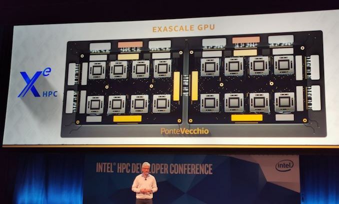
It has been a couple of weeks since Intel formally provided some high-level detail on its new discrete graphics strategy. The reason for the announcements and disclosures centered around Intel’s contract with the Department of Energy to build Aurora, an exascale supercomputer at the Argonne National Laboratory. The DoE and Argonne want developers clued into the hardware early, so when the supercomputer is deployed it can be used with as little ‘learning time’ as possible. This means Intel had to flesh out some of its strategy, as well as lift the lid on its first announced discrete GPU product. Only time will tell if it’s a bridge too far, or over troubled water, but today we know it as Ponte Vecchio.
Intel On Discrete Graphics: A Quick Recap
While Intel has had a graphics portfolio for a couple of decades, those graphics solutions have been limited to embedded graphics and integrated graphics solutions. There was a slight attempt to move into the graphics space and play with the big boys, with the Intel i740, however that was a long time ago. Intel’s current graphics architecture, called ‘Gen’, is currently in use in hundreds of millions of mobile devices, and is present in a substantial number of desktop processors, even if a discrete GPU is being used instead.
Intel has had high hopes for the graphics space before. Known as ‘Larrabee’, Intel attempted to engineer what was essentially x86 based graphics: using wide vector engines based on the same code path as Intel CPUs, the idea was to provide high-end graphics performance with the ease of programming in standard CPU code. While that product did actually run a number of graphics demos over the years, the hardware ended up being put to use in the high-performance computing market, where some developers saw the use of five-dozen 512-bit wide vector units absolutely fantastic for their simulations. This was the birth of AVX-512, which has lived on and now in Intel’s Xeon Scalable CPUs as well as consumer-grade Ice Lake laptop processors. The product that ‘Larrabee’ ended up as, Xeon Phi, scored a number of supercomputer wins and originally the Xeon Phi ‘Knights Hill’ product was destined to be put into Aurora in 2020. However the Xeon Phi program only lasted a few generations, with the final ‘Knights Mill’ hardware not being widely deployed and subsequently put to pasture.
Fast forward several years, and some management adjustments, and Intel has decided once again to enter the big graphics market. This time they’re going with something more conventional, something that looks more like a traditional graphics design. While the project started somewhere around three years ago, the big announcement that Intel was serious was when the company hired Raja Koduri, AMD’s Chief Graphics Architect in December 2017, and then Jim Keller, renowned SoC Guru. Raja Koduri’s title, Chief Architect, and his two decade of experience in building graphics solutions at AMD and Apple showcased how serious Intel was with this.
Since December 2017, Intel hasn’t said much about its new graphics plans. Under Ari Rauch, notable marketing figures and analysts were hired to be part of the team. Intel disclosed at its Architecture Day in December 2018 that the graphics solutions it would offer would be a full top-to-bottom implementation, covering low power integrated graphics all the way to the high-end. At the time Intel stated there would be two main GPU microarchitectures, all building from the ‘Xe’ architecture. Xe is meant to stand for ‘eXascale for Everyone’ (rather than x^2.718), with the marketing message that Intel wants to put high-end performance and efficiency anywhere it can.
As part of HPC DevCon, and Intel’s announcement with the DoE/Argonne, the veil was lifted, and we were told very slightly more than just the high level information. We were lucky enough to speak with Raja Koduri in a worldwide exclusive for the event, as his first official 1-on-1 interview since he joined Intel. It is worth a read and gives his perspective on a lot of ideas, as well as some of the decisions he has made.

This article is going to dive into Intel’s HPC DevCon disclosures about their graphics strategy. Here we are going to cover some of the blurb about Intel’s big plans, the new ‘third’ microarchitecture in Xe called Xe-HPC, the new GPU product ‘Ponte Vecchio’, Intel’s new Memory Fabric, a breakdown of the oneAPI software stack as presented, and what all this means for the rest of Intel’s graphics platform.
Exascale for Everyone
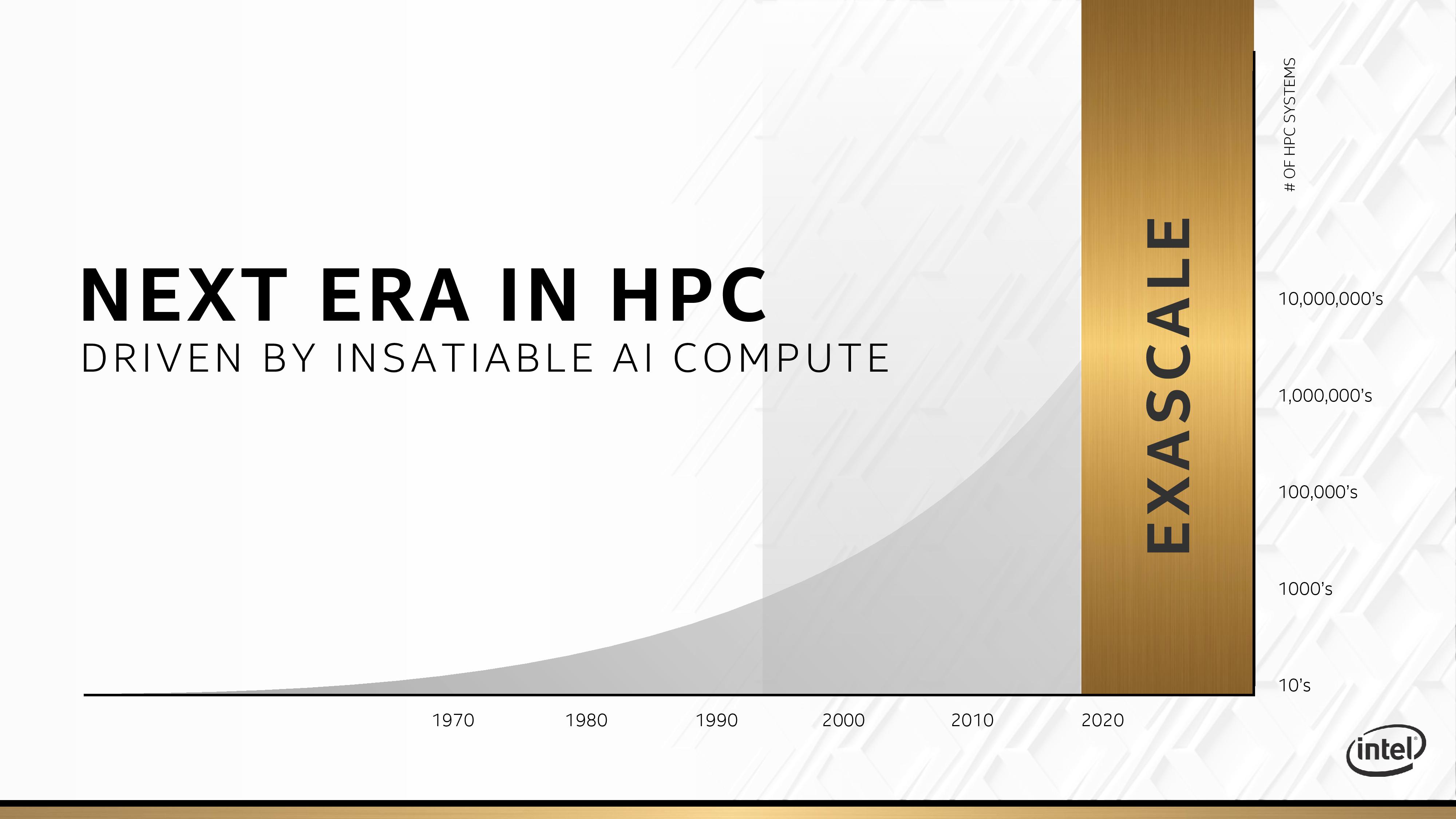
Intel says that it is hard not to notice the ‘insatiable’ demand for faster, more power efficient compute. Not only that, but certain people want that compute at scale, specifically at ‘exascale’. (It was disclosed at a high-performance supercomputing event, after all). For 2020 and beyond, Intel has designated this the ‘Exascale’ era in computing, where no amount of compute is good enough for leading edge research.
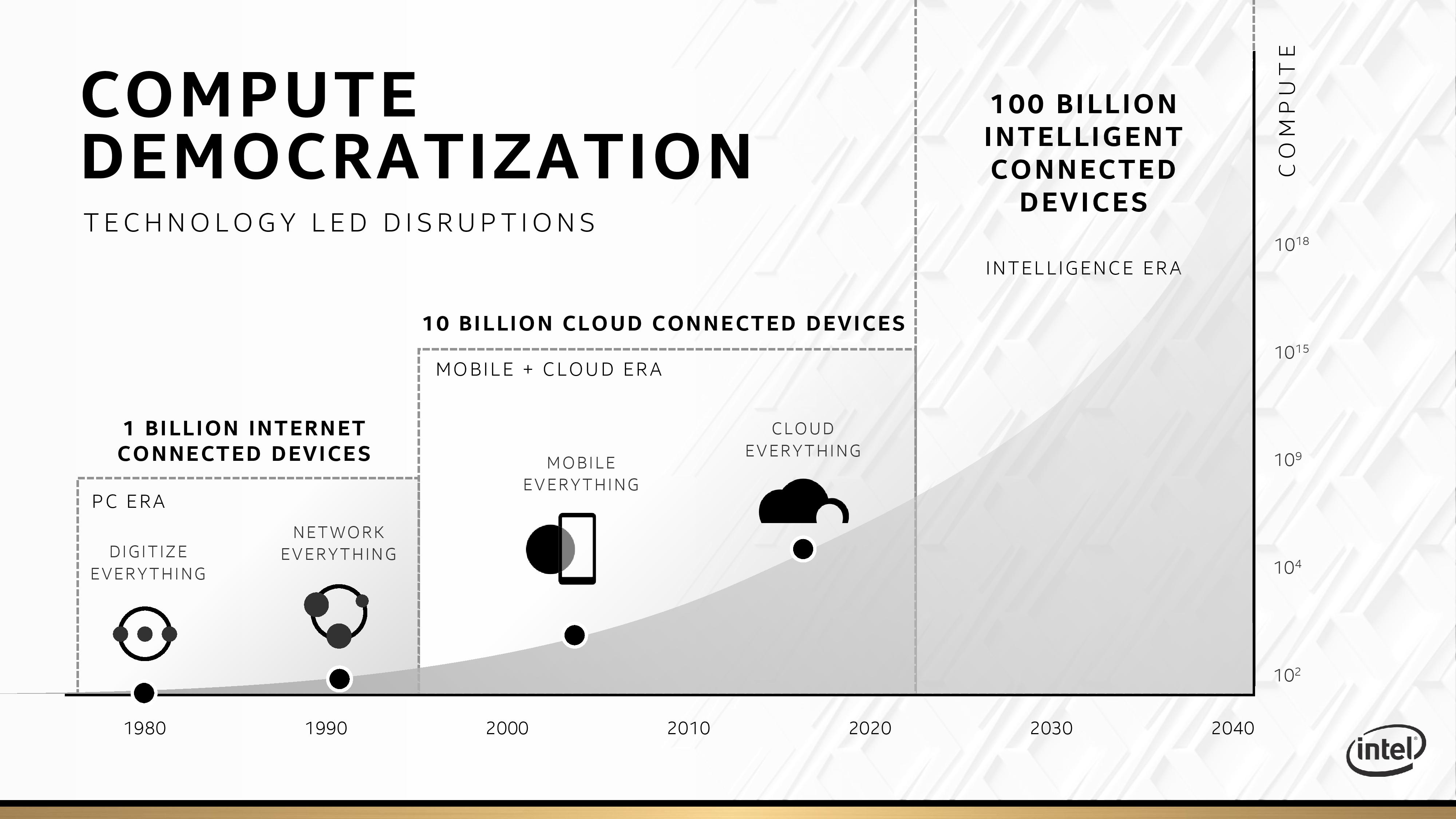
On top of this, Intel points to the number of connected devices in the market. A few years ago analysts were predicting 50 B IoT devices by 2020-2023, and in this presentation Intel is saying that by mid-2020 and beyond, there will be 100 billion devices that require some form of intelligent compute. The move to implementing AI, both in terms of training and inference, means that performance and computational ability have to be ubiquitous: beyond the network, beyond the mobile device, beyond the cloud. This is Intel’s vision of where the market is going to go.
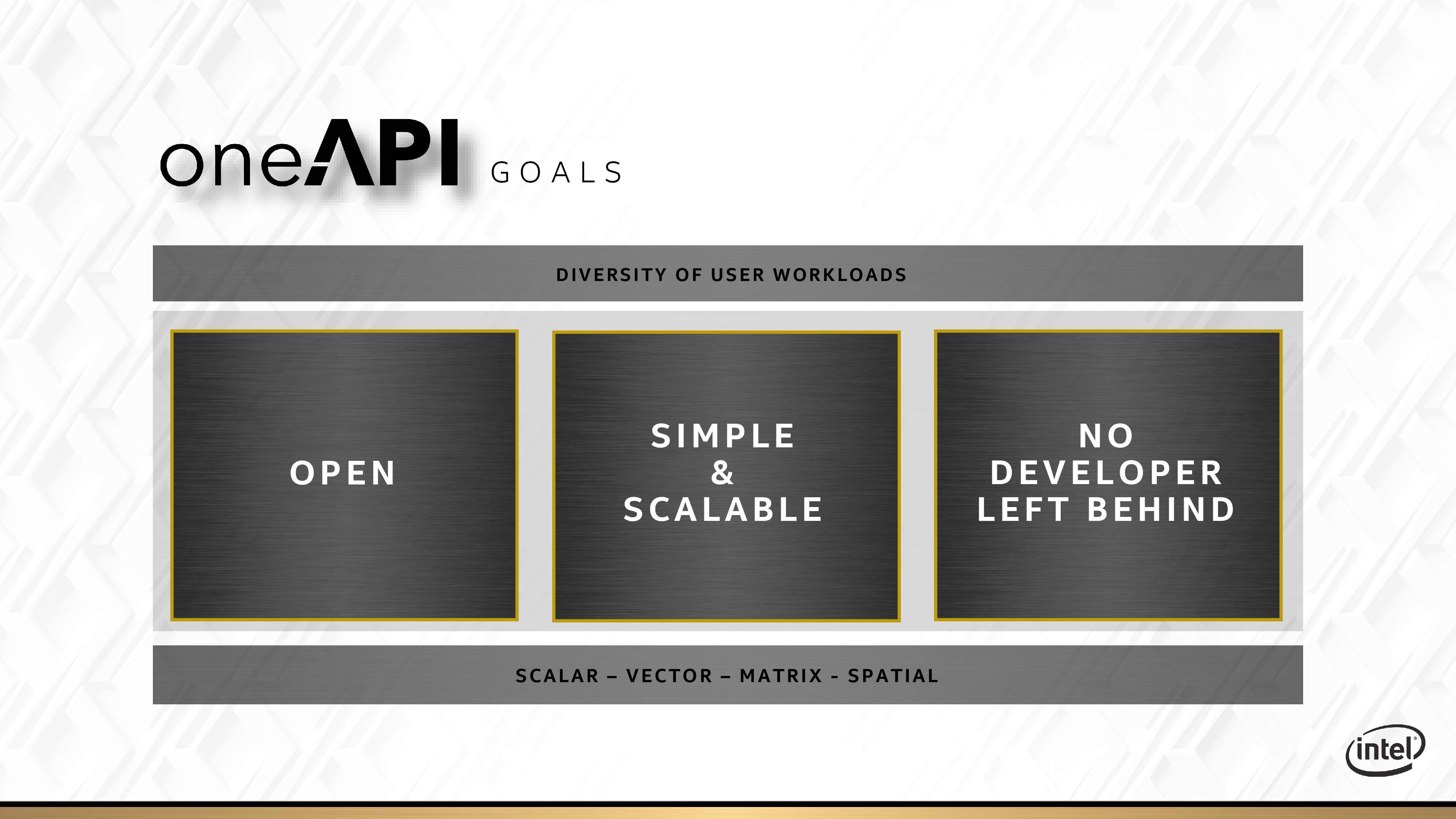
Intel splits this up into four specific categories of compute: Scalar, Vector, Matrix, and Spatial. This is certainly one blub part of the presentation I can say I agree with, having done high-performance programming in a previous career. Scalar compute, is the standard day-to-day compute that most systems run on. Vector compute is moving to parallel instructions, while Matrix compute is the talking point of the moment, with things like tensor cores and AI chips all working to optimize matrix throughput. The other part of the equation is spatial compute, which is derived from the FPGA market: for sparse compute that is complex and can be optimized with its own non-standard compute engine, then an FPGA solves it. Obviously Intel’s goal here is to cover each of these four corners with dedicated hardware: CPU for Scalar, GPU for Vector, AI for Matrix, and FPGA for Spatial.

One of the issues with hardware, as you move from CPU to FPGA, is that it becomes more and more specialized. A CPU for example can do Scalar, Vector, Matrix, and Spatial, in a pinch. It’s not going to be much good at some of those, and the power efficiency might be poor, but it can at least do them, as a launching point onto other things. With GPU, AI, and FPGA, these hardware specializations come with different amounts of complexity and a higher barrier to entry, but for those that can harness the hardware, large speed-ups are possible. In an effort to make compute more ubiquitous, Intel is pushing its oneAPI plan with a singular focal resource for all four types of hardware. More on this later.
Intel’s Xe architecture will be the underpinning for all of its GPU hardware. It represents a new fundamental redesign from its current graphics architecture, called ‘Gen’, and pulls in what the company has learned from products such as Larrabee/Xeon Phi, Atom, Core, Gen, and even Itanium (!). Intel officially disclosed that it has its first Xe silicon back from the fabs, and has performed power cycling and basic functionality testing with it, keen to promote that it is an actual thing.
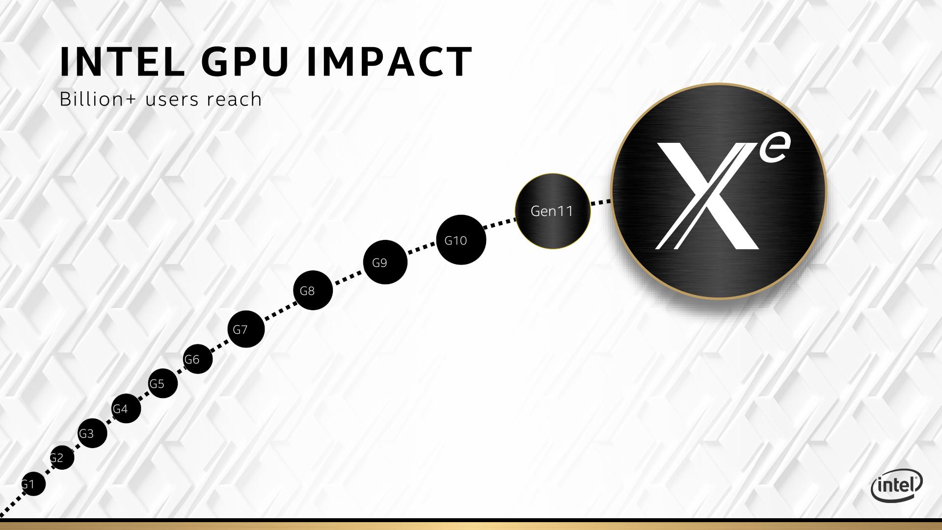
So far the latest ‘Gen’ graphics we have seen is the Gen11 graphics solution, which is on the newest Ice Lake consumer notebook processors. These are out in the market, ready to buy today, and feature performance 2x over the previous Gen9/Gen9.5 designs. (I should point out that Gen10 shipped in Cannon Lake but was disabled: this is the only graph ever where I’ve seen Intel officially acknowledge the existence of Gen10 graphics.) We have seen diagrams, either potentially from Intel or elsewhere, showing ‘Gen12’. It would appear that ‘Gen12’ was just a holding name for Xe, and doesn’t actually exist as an iteration of Gen. When we asked Raja Koduri about the future of Gen, he said that all the Gen developers are now working on Xe. There are still graphics updates to Gen, but the software developers that can be transferred to Xe have been already.
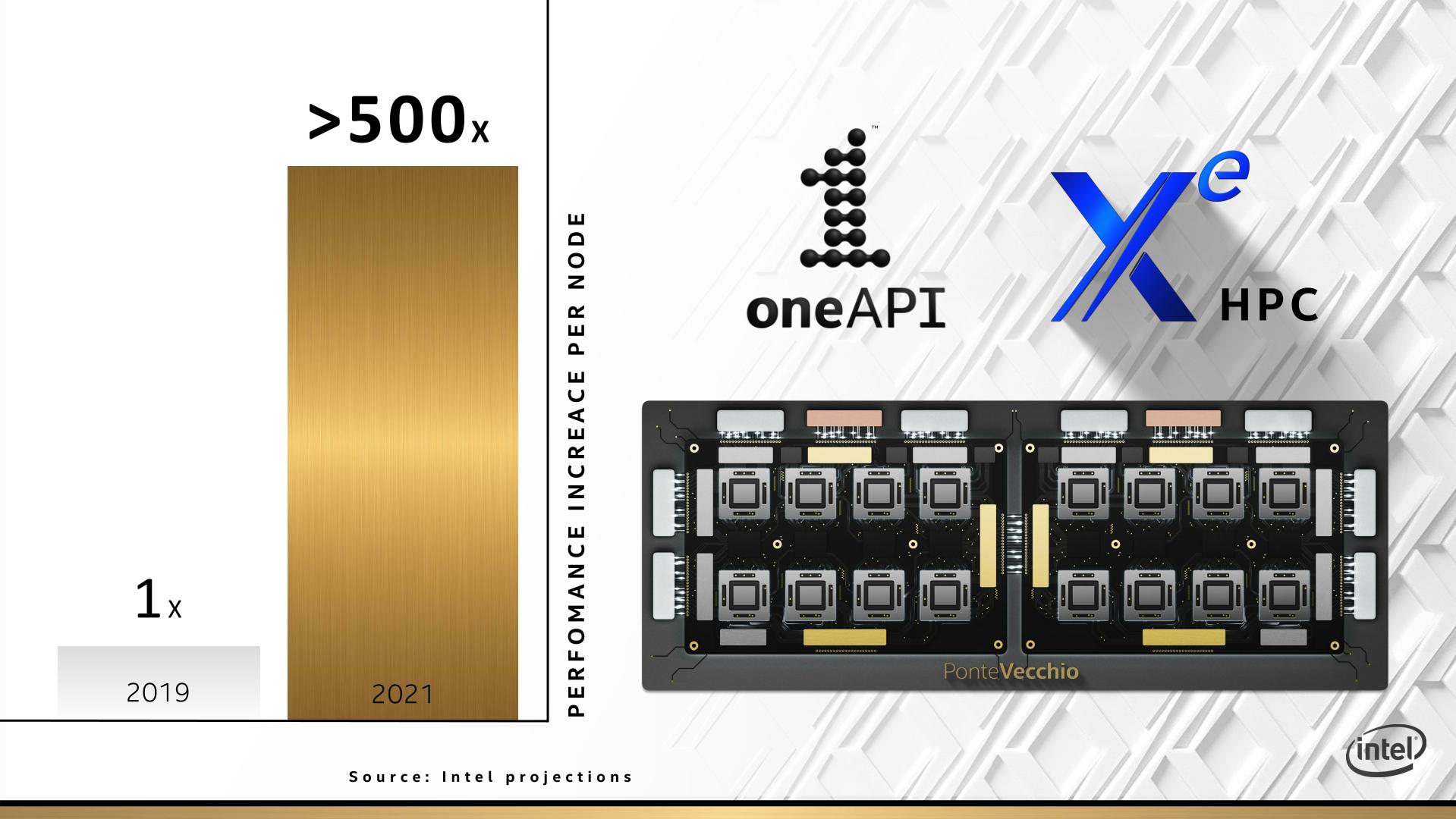
If you’re only going to read one thing today, then I want to skip ahead to Raja’s final slide of what he presented at HPC DevCon. Putting a quite ambitious goal in front of the audience, it showed that Intel wants to be able to provide a 500x in performance per server node by the end of 2021 compared to the per-node performance in 2019.
Now it is worth noting that this goal wasn’t specifically nailed down: are we comparing vector code running in scalar mode on a single 6-core Xeon Bronze in 2019 to an optimized dual-socket with six Xe GPUs in 2021? 500x is a big bet to make, so I hope Intel is ready.
In the next few pages, we’ll cover Xe, Ponte Vecchio, oneAPI, and Aurora.


47 Comments
View All Comments
MenhirMike - Tuesday, December 24, 2019 - link
This is way above the stuff I work with, but now I want RAMBO Cache on all my stuff.Batmeat - Tuesday, December 24, 2019 - link
How did he know I would do that?
Duncan Macdonald - Tuesday, December 24, 2019 - link
Given Intel's brilliant(!!!) success in getting its 10nm process to work, I would take the dates with a few megatons of salt!!!repoman27 - Wednesday, December 25, 2019 - link
Ian, I think your block diagram is a little off. Although the Intel illustrations clearly involve a certain amount of artistic license, I think we can agree that there's an organic package substrate with 8 HBM stacks and 2 transceiver tiles which are connected via EMIB to two larger modules. The modules appear to be a stack with two interposers sandwiched together. The bottom interposer has 8 large chips which are most likely the XeMF dies, as well as several color coded regions representing EMIB zones along with a bunch of vias. The top interposer has the 8 XeHPC chiplets and 4 additional chips which are almost certainly the RAMBO caches, seeing as they look exactly like the depiction of said caches in the other slide. Then there is one giant ball grid connecting the top and bottom layers of the sandwich.That looks an awful lot like Co-EMIB to me. The 7nm compute chiplets and SDRAM caches (built on whatever process is the best fit) are bonded directly (Foveros) to a wafer with the memory fabric dies (probably on 14nm) and riddled with TSVs. Those modules then get singulated and plunked onto a substrate with a bunch of EMIBs inserted into it which connect them to each other as well as to the HBM stacks and transceiver tiles.
Also, this point seems a little harsh: "Transition through DDR3 to DDR4 (and DDR5?) in that time frame". Intel may be way behind on their roadmap, but they made the transition to DDR4 several years ago with Skylake.
repoman27 - Wednesday, December 25, 2019 - link
In fact, Intel may have already shown off a prototype wafer of the modules themselves: https://pbs.twimg.com/media/D_C-9b3U0AAeyv7.jpgvia Anshel Sag on Twitter: https://twitter.com/anshelsag/status/1148627973882...
thetrashcanisfull - Wednesday, December 25, 2019 - link
This seems worryingly light on technical details with a lot of bold performance claims. Particularly the architectural stuffIf Intel really has managed to execute a proper chiplet style GPU with EMIB / chip stacking, that would certainly open the door to major performance uplifts, but they are staying super vague on the underlying architecture and topology. Honestly, this slideware feels reminiscent to 3D XPoint, which, while still a solid technology, was years late and never delivered on the sort of hype it was announced with.
I'll remain skeptical until we get more details - the advances in packaging and interconnects that Intel is touting could certainly enable improvements on this scale, but Intel's execution over the last decade leaves a lot of room for doubt.
smilingcrow - Wednesday, December 25, 2019 - link
'Intel's execution over the last decade leaves a lot of room for doubt.'Decade! I thought they were ahead of the pack generally until Zen 2 was released 18 months ago!
They have had a terrible 2 years but if you want to look at the last decade the real underachievers surely were AMD.
The next few years are crucial so we will have to see how things pan out.
thetrashcanisfull - Wednesday, December 25, 2019 - link
Decade may be an exaggeration, but not by much. Look at all of Intel's attempts to break into markets new markets: mobile/cellular, Larrabee/MIC, FPGAs (Altera), 3D XPoint...Intel has shown that it can be fairly successful as an incumbent in the server/desktop/laptop CPU market (or at least it could until the 10nm problems) but outside of that Intel has consistently struggled to deliver on anything over the last 8+ years.
jabber - Wednesday, December 25, 2019 - link
Maybe it could be said with AMD struggling they did let off the gas pedal a bit and coasted a while.thetrashcanisfull - Wednesday, December 25, 2019 - link
I think that's certainly true. Intergenerational improvements post Sandy Bridge were pretty anemic in the consumer market largely since intel refused to put out more than 4 cores on a mainstream platform until coffee lake. In the server/HEDT intel was doing pretty well for a while by virtue of increasing core counts, but the 10nm woes have halted any progress on that front.