Intel’s Manufacturing Roadmap from 2019 to 2029: Back Porting, 7nm, 5nm, 3nm, 2nm, and 1.4 nm
by Dr. Ian Cutress on December 11, 2019 3:00 PM EST
Update: After some emailing back and forth, we can confirm that the slide that Intel's partner ASML presented at the IEDM conference is actually an altered version of what Intel presented for the September 2019 source. ASML added animations to the slide such that the bottom row of dates correspond to specific nodes, however at the time we didn't spot these animations (neither did it seem did the rest of the press). It should be noted that the correlation that ASML made to exact node names isn't so much a stretch of the imagination to piece together, however it has been requested that we also add the original Intel slide to provide context to what Intel is saying compared to what was presented by ASML. Some of the wording in the article has changed to reflect this. Our analysis is still relevant.
One of the interesting disclosures here at the IEEE International Electron Devices Meeting (IEDM) has been around new and upcoming process node technologies. Almost every session so far this week has covered 7nm, 5nm, and 3nm processes (as the industry calls them). What we didn’t expect to see disclosed was an extended roadmap of Intel’s upcoming manufacturing processes. It should be noted that the slide presented at the conference by Intel's partner, ASML, was modified slightly from its original source.
They say a slide is worth 1000 words. Here’s 1000 words on Intel's future.
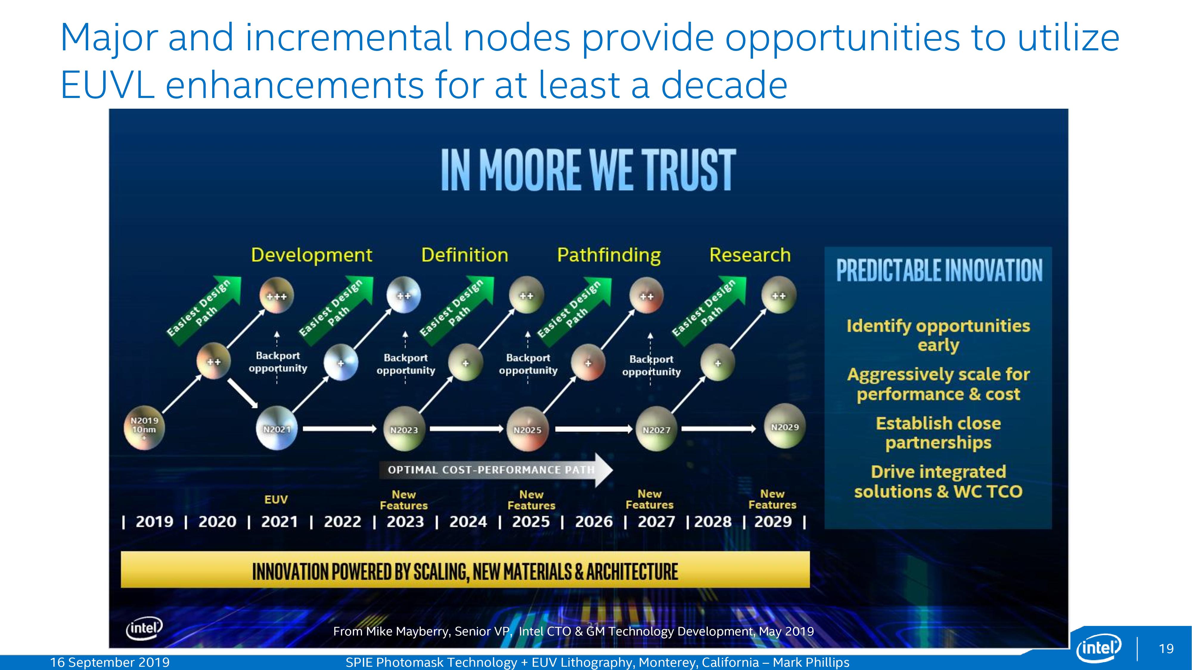
Intel's slide, as presented in September
This is Intel's original slide, not detailing which nodes in which years. However, it should be easy enough to figure out that each one of the elements in the bottom row is the next process node along, otherwise the +/++ wouldn't make sense.
ASML applied these assumptions to the slide it presented at the IEDM keynote, but the company did not disclose that they had modified the slide.
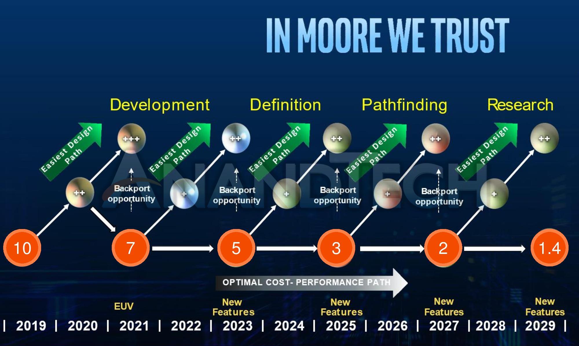
Intel's slide with ASML's animations overlayed, as shown in the slide deck distributed by ASML
So let’s go through some key areas.
1.4nm in 2029
Intel expects to be on 2 year cadence with its manufacturing process node technology, starting with 10nm in 2019 and moving to 7nm EUV in 2021, then a fundamental new node in each of 2023, 2025, 2027, 2029. This final node is what ASML has dubbed '1.4nm'. This is the first mention on 1.4nm in the context of Intel on any Intel-related slide. For context, if that 1.4nm is indicative of any actual feature, would be the equivalent of 12 silicon atoms across.
It is perhaps worth noting that some of the talks at this year’s IEDM features dimensions on the order of 0.3nm with what are called ‘2D self-assembly’ materials, so something this low isn’t unheard of, but it is unheard of in silicon. Obviously there are many issues going that small that Intel (and its partners) will have to overcome.
+, ++, and Back Porting
In between each process node, as Intel has stated before, there will be iterative + and ++ versions of each in order to extract performance from each process node. The only exception to this is 10nm, which is already on 10+, so we will see 10++ and 10+++ in 2020 and 2021 respectively. Intel believes they can do this on a yearly cadence, but also have overlapping teams to ensure that one full process node can overlap with another.
The interesting element to these slides is the mention of back porting. This is the ability for a chip to be designed with one process node in mind, but perhaps due to delays, can be remade on an older ‘++’ version of a process node in the same timeframe. Despite Intel stating that they are disaggregating chip design from process node technology, at some point there has to be a commitment to a process node in order to start the layouts in silicon. At that point the process node procedure is kind of locked, especially when it goes to mask creation.
In the slide, it shows that Intel is going to allow a workflow such that any first gen 7nm design could be back ported to 10+++, any first gen 5nm design could be back ported to 7++, and so on. One can argue that this roadmap might not be so strict with the dates – we have seen Intel’s 10nm take a long time to bake, so expecting the company to move with a yearly cadence on + updates alongside a two-year cadence with main process technology nodes would appear to be a very optimistic and aggressive cadence strategy.
Note that this isn’t the first mention of back porting hardware designs when it comes to Intel. With the current delays to Intel’s 10nm process technology, it has been widely rumoured that some of Intel’s future CPU microarchitecture designs, originally designed with 10nm (or 10+, 10++) in mind might actually find a home on a 14nm process due to the success of that process node.
Development and Research
Normally with process node developments, there will be different teams working on each process node. This slide states that Intel is currently in development of its 10+++ optimizations as well as the 7nm family. The idea is that the ‘+’ updates are capturing the low hanging fruit from a design standpoint every generation, and the number represents a full node benefit. Interestingly we see Intel’s 7nm being based on 10++, whereas in the future Intel sees 5nm come from the base 7nm design, and 3nm coming from 5nm. There is no doubt that some of the optimizations that enter each +/++ update will filter into future designs as and when they are needed.
In this slide, we have Intel’s 2023 node currently in the definition stage. At this IEDM conference there’s a lot of talk about 5nm in this timeframe, so some of those improvements (such as manufacturing, materials, consistency, etc.) will ultimately end up in Intel’s process depending on which design houses they partner with (historically Applied Materials). It is worth noting that 5nm is listed as a 2023 node, which is around the time that ASML will start selling its ‘High NA’ EUV machines to help with better path definition during the manufacturing process. I’m not sure if High NA will intercept at 5nm or 3nm, assuming this Intel roadmap has its dates correct and Intel is able to stick to it, but it is something to consider
Beyond 2023, Intel is currently in the ‘path-finding’ and 'research' mode. As always when looking this far out, Intel is considering new materials, new transistor designs, and such. At this IEDM conference we’re seeing a lot of talk of gate-all-around transistors, either as nano-sheets or nano-wires, so no doubt we’re going to see some of that as FinFET runs out of steam. TSMC is still using FinFETs for its 5nm process (Intel’s 7nm equivalent), so I wouldn’t be surprised if we see something like nano-sheets then nano-wires (or even hybrid designs) come into Intel’s manufacturing stack.
It’s worth also pointing out, based on the title of this slide, that Intel still believes in Moore’s Law. Just don’t ask how much it’ll cost.


138 Comments
View All Comments
Ian Cutress - Tuesday, December 10, 2019 - link
There is an element of that, a sort of cooperative DTCO between techniques to help improve older process node technologies. However as the graph shows, the new node is derived from the first gen of the previous node, so how much can be back-ported on the litho side is perhaps questionable.anonomouse - Wednesday, December 11, 2019 - link
They've definitely done things like this in the past. For example, 22FFL took the transistor fin from their 14nm, brought a modified version of a 14nm SRAM cell to 22FFL as the HCC SRAM, and those are just the things they publicly talked about. I'm sure there are other things they could bring over as well, like adaptations in the via/metal layers with new materials or modified double-damascene etc etc etc.What I think everyone here is jumping to for 'backporting' is assuming this means Sunny Cove or Willow Cove etc being brought a process node. Nothing in any of these materials suggests that at all.
versesuvius - Wednesday, December 11, 2019 - link
Roughly speaking (n) nano meters is still the same no matter what technology is used to make it (i.e. same transistor count per area, hence the same power use). It will mean better yields, which in turn means lower supply of low end chips (i3, pentium, celeron) and some low volume weirdos. Improving architecture and design is a different matter, which until now was not called backporting but it is now.peevee - Tuesday, December 10, 2019 - link
Somebody please sue them all for the fraudulent names.milkywayer - Tuesday, December 10, 2019 - link
There should be jail time for such BS but it should apply to the top management. Enough of these fake nm and fake unlimited cell phone plans.CiccioB - Tuesday, December 10, 2019 - link
The backport opportunity just shows a underline problems of the future PPs: costs.Complexity and design costs will just have an great impact on the choice of the PP to chose, and seeing that since 22nm transistor/cost curve has turned negative, it is even possible that for the next PPs, when you are not forced to use the latest shiny expensive new PP for performance/consumption issues, you may get cheaper designs using older PP.
MCM designs will also help in reducing the needs of smaller transistors at all costs.
candre23 - Tuesday, December 10, 2019 - link
It's a bit of a stretch to claim that they're "already on" 10nm, considering they've only managed to actually ship a handful of mobile parts on that process node. Intel has been stuck on 14nm for nearly six years and is *still* struggling to manage decent enough yields on 10nm to actually sell them. Are we really to believe that they're capable of a node shrink every other year - especially when each further shrink is going to be harder than the last?This is just intel trying to salvage some industry faith after getting hammered by AMD for the last couple years.
nevcairiel - Wednesday, December 11, 2019 - link
10nm was broken, but 7nm is an entirely different process using EUV. As long as they kept development of it active, the 10nm problems should not really impact it.7nm EUV is realistically easier to do then the 10nm process, since EUV solves many of the problems that a small DUV process had to overcome.
Santoval - Wednesday, December 11, 2019 - link
EUV is not exactly the holy grail of photolithography. It solves plenty of DUV's problems (largely because the much tighter wavelength can let fabs etch patterns in just one step instead of 2 to 4 steps) but it has its own set of problems : high LER (Line Edge Rougness) of features, the step & scan machines have much lower energy efficiency (resulting in quite higher energy bills) due to much higher losses of EUV light from the source to the target, the optics need to be orders of magnitude more precise and are thus (also) far more expensive, and more or less the same applies to the masks and their pellicles, both of which need to be highly reflective (at least 85 - 90%).In short EUV is a much more delicate, elaborate, and *far* more expensive business than DUV, which my guess is what forced GloFo to bow down from the EUV game. Intel, TSMC and Samsung have the monies to invest in EUV R&D and build EUV fabs with many ASML's EUV scanners, but I strongly doubt anyone else can do it. As for manufacturers of EUV scanners ASML will almost certainly remain the only company in the world in the future as well. Their monopoly naturally allows them to charge whatever they think the trio of companies above can afford to pay, nothing less and nothing more.
CiccioB - Thursday, December 12, 2019 - link
AFAIK, EUV is more expensive for each mask, but it requires less masks than DUV.That's why TSMC 7nm+ PP is looked for lowering production costs and raise the yields, as all those multiple patterning processes will no be needed anymore.
Probably he big drawbacks of EUV is that is is slower to produce. So it needs more scanner, or faster more expensive ones. And that's also why EUV is not applied to all layers in its first version, but only on the critical ones that on multipatterning raise DUV costs and lower yields..