A Big Bet on SOI: GlobalFoundries Preps Another Supply Agreement for 300mm SOI Wafers
by Anton Shilov on February 27, 2020 5:30 PM EST- Posted in
- Semiconductors
- GlobalFoundries
- FD-SOI
- RF SOI
- Soitec
- SOI
- GlobalWafers
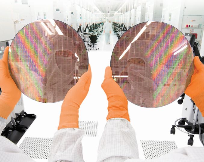
Having dropped out of the race for leading-edge manufacturing technologies in order to focus on specialty fabrication processes, GlobalFoundries has pinned some big hopes in manufacturing RF-SOI chips for various 5G applications, as well as FD-SOI chips for low-power devices. This week the company signed a memorandum of understanding (MOU) with GlobalWafers Co. (GWC) to develop a long-term supply contract for 300 mm SOI wafers, GloFo's second long-term SOI wafers supply agreement (WSA) in less than a year.
Once primarily used to build leading-edge processors, silicon-on-insulator (SOI) technology is used today for a wide variety of applications, including those that need an ultra-low power consumption (SoCs and MCUs for IoT applications), high voltages (analog/mixed signal), or high resistivity (4G and 5G front-end modules [FEMs] for smartphones). All of these are made using so-called specialty manufacturing technologies, and to that end they are of tremendous interest for GlobalFoundries. Meanwhile, considering the rise of 5G and IoT, RF-SOI and FD-SOI are the most promising technologies when it comes to producing the necessary chips in high volumes.

Nowadays, GlobalFoundries operates seven fabs: four 300-mm fabs (including the Fab 10 in East Fishkill, New York) and three 200-mm fabs. The company’s largest 300-mm Fab, Fab 1, is used exclusively to make SOI products, Fab 7 in Singapore uses both bulk and SOI technologies, and Fab 10 can also process wafers using SOI-based processes. In addition, GlobalFoundries is building another 300-mm fab in Chengdu, China, which will also be used to make chips using its 22FDX technology. Finally, the foundry’s 200-mm facilities can all use SOI wafers as well.
Being the largest consumer of SOI wafers in the world, GlobalFoundries sources 200-mm and 300-mm substrates from both Soitec, the world’s largest producer of SOI wafers, as well as GlobalWafers Co. In fact, in just the last year GloFo and Soitec signed a multi-year 300-mm SOI wafer supply agreement, which builds upon a WSA signed in 2017. As it turns out, GlobalFoundries needs even more 300-mm SOI wafers for its advanced RF SOI technologies, so the company is going as far as agreeing to help GWC ‘significantly expand’ its SOI wafer manufacturing capacity as part of the new contract.
GlobalFoundries, Soitec, and GlobalWafers Co. naturally do not disclose how many wafers are consumed by the chip maker. Regardless, it looks like we are talking about a significant expansion of SOI usage at GlobalFoundries.
Bami Bastani, senior vice president for mobile and wireless infrastructure at GlobalFoundries:
“Mobile, wireless, and 5G represent a significant opportunity for GlobalFoundries, and our vital RF technology is featured in more than 85% of smartphones on the market today. We are pleased to collaborate with GlobalWafers, and look forward to working with them to develop and qualify an additional supply of 300mm SOI wafers to integrate into our manufacturing processes and help meet the growing demand for our RF SOI solutions.”
Tom Weber, senior vice president and chief procurement officer at GlobalFoundries said the following:
“Given our market position, it is in our best interest – and the best interest of our clients – to build out and diversify the supply chain for 300mm SOI wafers. GlobalWafers is the right partner for us to make this happen.”
Related Reading:
- GlobalFoundries Stops All 7nm Development: Opts To Focus on Specialized Processes
- GlobalFoundries Weds FinFET and SOI in 14HP Process Tech for IBM z14 CPUs
- GlobalFoundries to Expand Capacities, Build a Fab in China
- GlobalFoundries and Chinese Authorities Reconsider Plans
- GlobalFoundries Enables Connectivity IP: New RF SOI and Ensigma BLE on 22FDX
Source: GlobalFoundries


26 Comments
View All Comments
eastcoast_pete - Friday, February 28, 2020 - link
Are these 300 mm wafers to be used for GloFo's 12 nm FDSOI (fully-depleted silicon on insulator)? The article (apparently from a press release) omits any details on that. At least one of the Fabs named was retrofitted for 12 nm FDSOI, which is supposed to be especially power efficient. Some information on that power efficiency would be great, too!Dragonstongue - Friday, February 28, 2020 - link
ROFL...I can only "assume" most folks who come to sites such as this absolutely KNOW what SOI is, as others have pointed out, maybe some "not known" other abbreviations it would be helpful, but SOI has been a VERY long time in use decade+ is anything but a "new term"..I myself do not get the "undies in a bunch" commentary, upset because? did not spell out what SOI stands for till a few sentences in..does it REALLY MATTER?
Ii would be picking more upon when product announcement is given (to them, from the makers) but does not include things such as battery size, if there is 3.5mm jack, type of power connectors, P/E cycles and such things.
but not IMHO for such a silly thing as SOI..that is my .02c
GreenReaper - Friday, February 28, 2020 - link
FWIW, I'm a computer geek, not a silicon geek. I would've guessed silicon-on-interposer, not insulator, because interposers are talked about frequently with relation to silicon chip substrates.People are getting up in arms about things that would normally be covered by an sub-editor, and they are not seeing them here - such inconsistencies suggests that normal phase is missing.
andrewaggb - Friday, February 28, 2020 - link
SOI was all the rage for most of the 2000's. People following tech news during those years should know it well but after that it's pretty understandable that people don't necessarily know what it is.dotjaz - Friday, February 28, 2020 - link
What an ignorant comment! You can't assume people in their 20s would know SOI. The last time SOI making waves it was mid-2000s, by the time 45nm SOI hit the market, we already know there won't be a 28nm and smaller node for the decade to come. People get into technology world in the 2010s won't necessarily know what it is from bits and pieces reported about 28FDS 22FDX 14HP 12FDX.haukionkannel - Friday, February 28, 2020 - link
Most likely next gen Zen3 cpus have these in IO chip part and clobal foundaries Expect to be selling those a lot!