SK Hynix: HBM2E Memory Now in Mass Production
by Ryan Smith on July 2, 2020 10:00 AM EST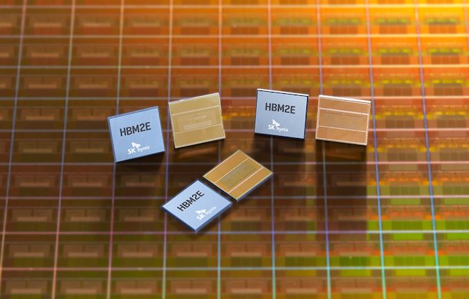
Just shy of a year ago, SK Hynix threw their hat into the ring, as it were, by becoming the second company to announce memory based on the HBM2E standard. Now the company has announced that their improved high-speed, high density memory has gone into mass production, offering transfer rates up to 3.6 Gbps/pin, and capacities of up to 16GB per stack.
As a quick refresher, HBM2E is a small update to the HBM2 standard to improve its performance, serving as a mid-generational kicker of sorts to allow for higher clockspeeds, higher densities (up to 24GB with 12 layers), and the underlying changes that are required to make those happen. Samsung was the first memory vendor to ship HBM2E with their 16GB/stack Flashbolt memory, which runs at up to 3.2 Gbps in-spec (or 4.2 Gbps out-of-spec). This in turn has led to Samsung becoming the principal memory partner for NVIDIA’s recently-launched A100 accelerator, which was launched using Samsung’s Flashbolt memory.
Today’s announcement by SK Hynix means that the rest of the HBM2E ecosystem is taking shape, and that chipmakers will soon have access to a second supplier for the speedy memory. As per SK Hynix’s initial announcement last year, their new HBM2E memory comes in 8-Hi, 16GB stacks, which is twice the capacity of their earlier HBM2 memory. Meanwhile, the memory is able to clock at up to 3.6 Gbps/pin, which is actually faster than the “just” 3.2 Gbps/pin that the official HBM2E spec tops out at. So like Samsung’s Flashbolt memory, it would seem that the 3.6 Gbps data rate is essentially an optional out-of-spec mode for chipmakers who have HBM2E memory controllers that can keep up with the memory.
At those top speeds, this gives a single 1024-pin stack a total of 460GB/sec of memory bandwidth, which rivals (or exceeds) most video cards today. And for more advanced devices which employ multiple stacks (e.g. server GPUs), this means a 6-stack configuration could reach as high as 2.76TB/sec of memory bandwidth, a massive amount by any measure.
Finally, for the moment SK Hynix isn’t announcing any customers, but the company expects the new memory to be used on “next-generation AI (Artificial Intelligence) systems including Deep Learning Accelerator and High-Performance Computing.” An eventual second-source for NVIDIA’s A100 would be among the most immediate use cases for the new memory, though NVIDIA is far from the only vendor to use HBM2. If anything, SK Hynix is typically very close to AMD, who is due to launch some new server GPUs over the next year for use in supercomputers and other HPC systems. So one way or another, the era of HBM2E is quickly ramping up, as more and more high-end processors are set to be introduced using the faster memory.
Source: SK Hynix


37 Comments
View All Comments
Ryan Smith - Thursday, July 2, 2020 - link
Well that's embarrassing for a professional writer...Thanks!
eastcoast_pete - Friday, July 3, 2020 - link
Good! HBM memory (as HBM2, 2E) allows for more robust dGPUs in portable, such as laptops, due to its lower power draw. Just look at the most recent MacBook Pro with dGPU. AFAIK, it also has lower latencies than other VRAM, which makes it interesting for CPU use also, although that will probably stay reserved for server and high-end workstation use.anad0commenter - Friday, July 3, 2020 - link
Yes! This is what people don't get. HMB memory would be amazing for laptop sized GPUs. Nvidia produces multiple laptop SKUs of the same chip for different cases (there's at least 4 different mobile RTX 2080 variants). There's the Max Q versions, which are about a tier below their desktop counterparts, and then there's the full powered versions which are much closer to their desktop monikers (there's also multiple inbetween versions that are power starved by OEMs for thermal reasons and thus perform nowhere near their tier, but still cost the same)!HBM on mobile GPUs on the die itself would save on space in the laptop, heat generation, as well as power usage! The only downside is the cost of the chips... and unfortunately, that's a big big downside, especially for people who know nothing about laptops and are not ready to pay through the nose for something they don't understand.
Deicidium369 - Sunday, July 5, 2020 - link
Or it's a horrible idea and people know what they want. I would vote for the horrible idea theory.Smell This - Sunday, July 5, 2020 - link
Make me wonder if *Deicidium369* is the same Troll as *H-Stewart* and *Phynez* ...
JoeDuarte - Tuesday, July 7, 2020 - link
Anyone have a ballpark of how much this stuff costs, either from Samsung or SK Hynix? Or what regular HBM2 goes for these days?What about latency? How does HBM2(E) latency compare to DDR4 or GDDR6, from processor to memory? Does this stack configuration reduce latency?
Oxford Guy - Wednesday, July 8, 2020 - link
"What about latency?"I was going to ask the same thing.