TSMC’s Version of EMIB is ‘LSI’: Currently in Pre-Qualification
by Andrei Frumusanu on August 25, 2020 2:00 PM EST
Whilst process node technologies and Moore’s Law are slowing down, manufacturers and chip designers are looking to new creative solutions to further enable device and performance scaling. Advanced packaging technologies are one such area where we’ve seen tremendous innovations over the past few years, such as the introduction of silicon interposers and integration of HBM-memory or the shift towards modularisation through chiplet designs.
Silicon interposers pose cost challenges as they are expensive and require quite a large silicon footprint, whilst chiplet designs which use conventional packaging on organic substrates are limited by I/O bandwidth and power efficiency. A solution to this problem has been the industry’s introduction of intermediary silicon dies that connect two logic chips together – but only in a limited scope, not using the same footprint as a full silicon interposer. Intel’s EMIB (Embedded Die Interconnect Bridge) has been the recently most talked about implementation of such technology.
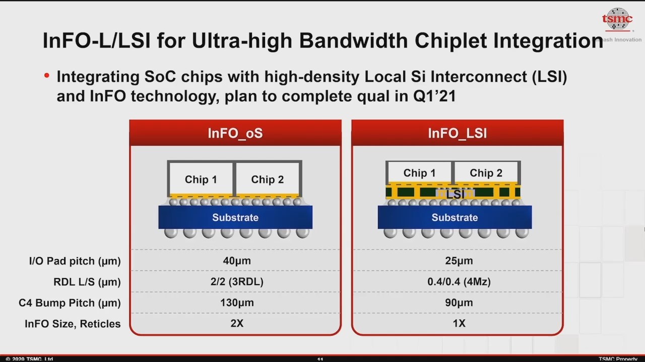
Today as TSMC’s 2020 Technology Symposium, the Taiwanese manufacturer is detailing their own variant of such a technology, called Local Si Interconnect (LSI), that will be offered for both InFO and CoWoS packaging technologies in the form of InFO-L and CoWoS-L.
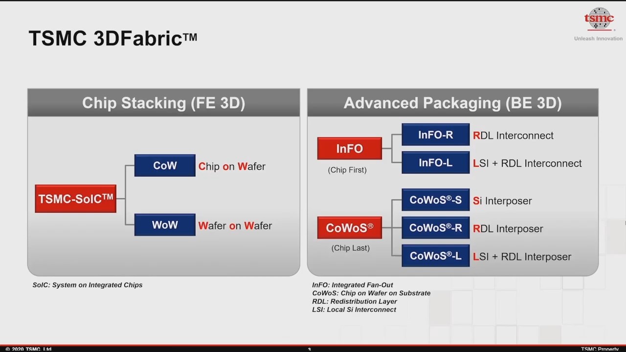
The new advancements are part of what TSMC now dubs its 3DFabric packaging technology platform which offers a versatile repertoire of integration and packaging options, which include SoIC, InFO, and CoWoS.
A brief explanation for our readers unfamiliar with the terms, SoIC (System on Integrated Chip) is TSMC’s bump-less chip stacking and hybrid bonding integration technology that allows for stacking multiple chip dies together, enabling extremely high-bandwidth and low power bonding between the silicon dies. Currently, this technology has no equal in the industry.
InFO is TSMC’s fan-out packaging technology, where a silicon die from a wafer is picked out and placed on a carrier wafer, upon which the further bigger structures such as the copper RDL (Redistribution layer), and later the carrier substrate is built upon.
TSMC’s variant of InFO with integration of an LSI is called InFO-L or InFO-LSI, and follows a similar structure with the new addition of it integrating this new local silicon interconnect intermediary chip for communication between two chips.
TSMC’s CoWoS (Chip-on-Wafer-on-Substrate) was originally described as the company’s silicon interposer 2.5D packaging technology, which is currently still falls under the CoWoS-S specifier, but meanwhile it also covers other chip-last packaging technologies. As the description hits it at, here the base substrate, RDL are built first, and only as the last step is the target silicon chip bonded to the package.
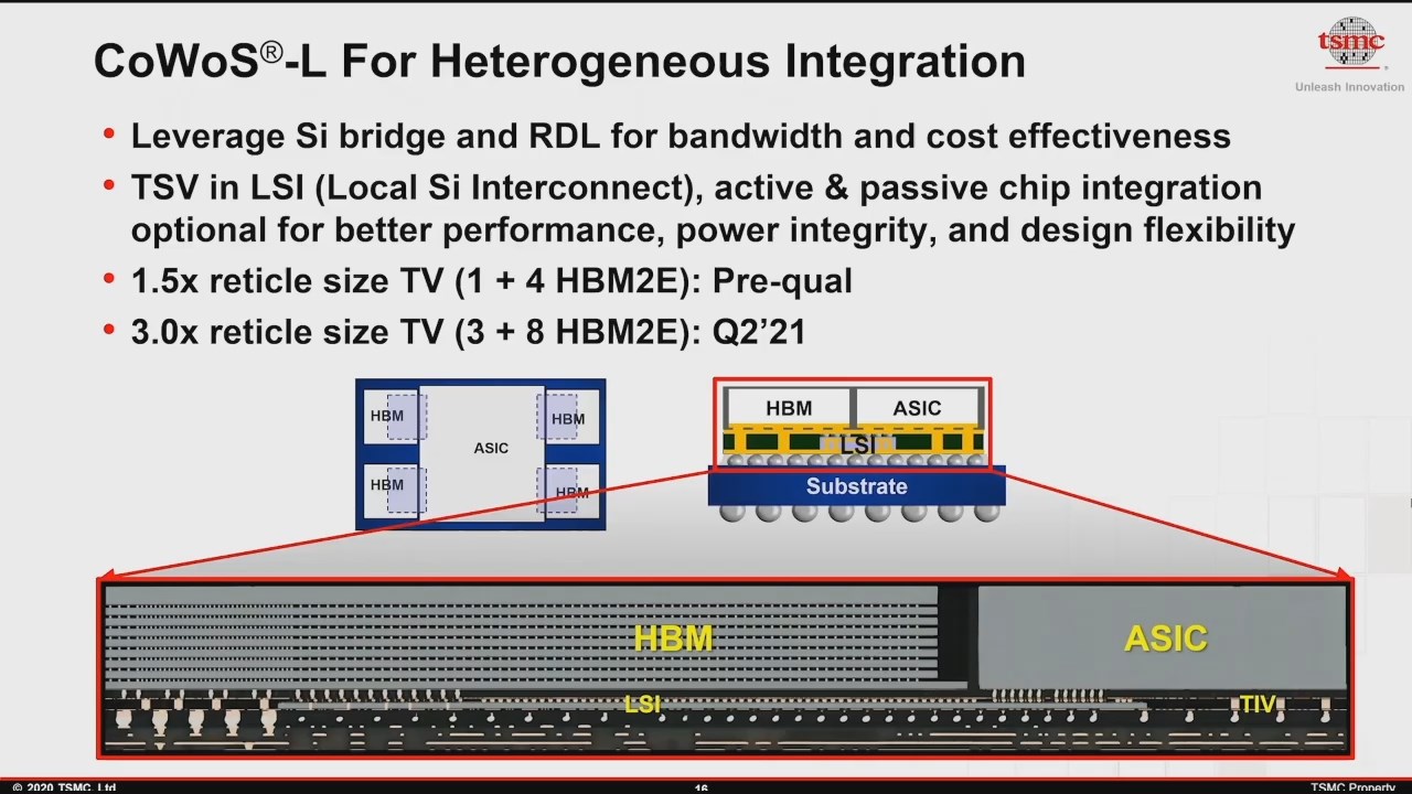
CoWoS-L is the new variant of TSMC’s chip-last packaging technology which adds in the Local Si Interconnect which is used in combination of a copper RDL to achieve higher bandwidth than just an RDL packaging implementation (CoWoS-R), and be more cost-effective than a full silicon interposer implementation (CoWoS-S).
TSMC describes the LSI as being either an active, or a passive chip, depending on chip designers needs and their cost sensitivities. The foundry expects to complete InFO-L qualification in Q1’21, and CoWoS-L is undergoing pre-qualification right now. Silicon bridge interconnect technologies such as LSI and EMIB are expected to bring high-performance chip designs at a lower cost for the designer and the consumer.
Related Reading
- TSMC Details 3nm Process Technology: Full Node Scaling for 2H22 Volume Production
- TSMC To Build 5nm Fab In Arizona, Set To Come Online In 2024
- TSMC & Broadcom Develop 1,700 mm2 CoWoS Interposer: 2X Larger Than Reticles
- TSMC Boosts CapEx by $1 Billion, Expects N5 Node to Be Major Success
- Early TSMC 5nm Test Chip Yields 80%, HVM Coming in H1 2020
- TSMC: 5nm on Track for Q2 2020 HVM, Will Ramp Faster Than 7nm
- TSMC: N7+ EUV Process Technology in High Volume, 6nm (N6) Coming Soon


17 Comments
View All Comments
Valantar - Wednesday, August 26, 2020 - link
Hm, I thought EMIB embedded _into_ the substrate, not into a layer on top of the substrate. Have I misunderstood this all along?anonomouse - Sunday, August 30, 2020 - link
You're correct, this is different. Here the local silicon appears to be integrated with the RDL.psychobriggsy - Wednesday, August 26, 2020 - link
It's good that a smaller silicon interconnect option is becoming available at TSMC. The large silicon interposers never came down in price it seems.TSMC have a lot of information here, that still might not clear everything up:
https://3dfabric.tsmc.com/english/dedicatedFoundry...
CoWoS-S doesn't really get described well. It might be a chip-sized RDL just to aid I/O placement+routing on the chip before it is attached to the substrate. RDLs are very thin because of the TSVs.
What we know as a standard interposer (logic+hbm typically): CoWoS-R (R=redistribution layer, with 6 layers of routing in the interposer). Multiple chips are attached to the interposer when it's on the wafer. The wafer is then thinned to expose TSVs and become quite thin, then it is cut and assembled to the substrate.
This article is about CoWoS-L - and besides the LSI bridges, it has *LOTS* of tiny thin RDLs hosted in a 'molding' which itself has through interposer vias. The LSI is mounted to the substrate using CoWoS-S, the TIVs and their small RDLs are also assembled, the molding is added, then the main logic dies on top. The LSI may contain active logic. LSI is thicker than RDL.
psychobriggsy - Wednesday, August 26, 2020 - link
Ugh, need an edit function here.-S is what I wrote as -R with the thin Si interposer and chip-first assembly.
-R is the version using an RDL, which is an organic interposer: https://semiengineering.com/return-of-the-organic-... (so calling it Chip *on Wafer* on Substrate is not really correct here. Should be CoRoS. Anyway, this is chip-last.
Andrei Frumusanu - Wednesday, August 26, 2020 - link
CoWoS-S is just using a standard interposer and no RDL whatsoever;> What we know as a standard interposer (logic+hbm typically): CoWoS-R
No, incorrect. There's no interposer at all here. I'm not aware of talked about -R products that I could use as an example.
> The LSI is mounted to the substrate using CoWoS-S
That sentence makes no sense. -S describes the use of an interposer, which is not present in -L.
psychobriggsy - Wednesday, August 26, 2020 - link
Thanks, yes I corrected myself above for the descriptions. One issue is that CoWoS-R is actually missing the "oW' part, it's 'oR' but I guess they didn't want to confuse branding any more than it is already confusing to outsiders. It sounds to me that RDLs will cut prices a lot for this type of packaging.I meant to write but messed it up (tiredness) "mounted to the substrate in a compatible manner to CoWoS-S" as TSMC's website mentions - the compatibility will aid uptake I'm sure.
rchidambaram - Wednesday, August 26, 2020 - link
If the LSI die has TSVs (needed to uBump on the bottom), seems more like Intel's Foveros than EMIB. As far as I know, EMIB does not have TSVs. Plus EMIB is embedded in a substrate and not in epoxy. The TIVs are similar to Intel's Omni Directional Interconnect (ODI).