Qualcomm's Cloud AI 100 Now Sampling: Up to 400TOPs at 75W
by Andrei Frumusanu on September 16, 2020 9:30 AM EST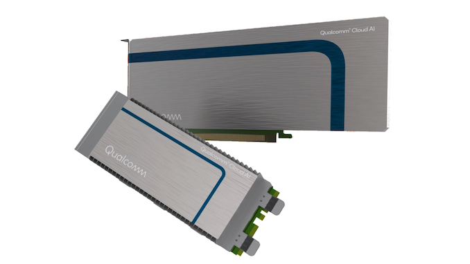
Today Qualcomm is revealing more information on last year’s announced “Cloud AI 100” inference chip and platform. The new inference platform by the company is said to have entered production already with the first silicon successfully coming back, and with first customer sampling having started.
The Cloud AI 100 is Qualcomm’s first foray into the datacentre AI inference accelerator business, representing the company’s investments into machine learning and leveraging their expertise in the area from the consumer mobile SoC world, and bringing it to the enterprise market. Qualcomm had first revealed the Cloud AI 100 early last year, although admittedly this was more of a paper launch rather than a disclosure of what the hardware actually brought to the table.
Today, with actual silicon in the lab, Qualcomm is divulging more details about the architecture and performance and power targets of the inferencing design.
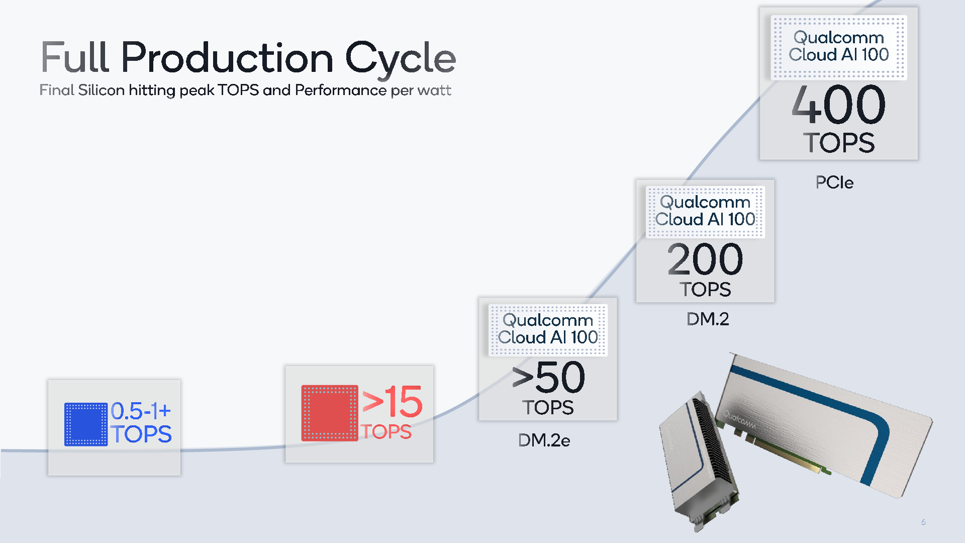
Starting off at a high-level, Qualcomm is presenting us with the various performance targets that the Cloud AI 100 chip is meant to achieve in its various form-factor deployments.
Qualcomm is aiming three different form-factors in terms of commercialisation of the solution: A full-blown PCIe form-factor accelerator card which is meant to achieve up to an astounding 400TOPs inference performance at 75W TDP, and two DM.2 and DM.2e form-factor cards with respectively 25W and 15W TDPs. The DM2 form-factor is akin to two M.2 connectors next to each other and gaining popularity in the enterprise market, with the DM.2e design representing a smaller and lower-power thermal envelope form-factor.
Qualcomm explains that from an architecture perspective, the design follows the learnings gained from the company’s neural processing units that it had deployed in the mobile Snapdragon SoC, however is still a distinct architecture that’s been designed from the ground up, optimised for enterprise workloads.
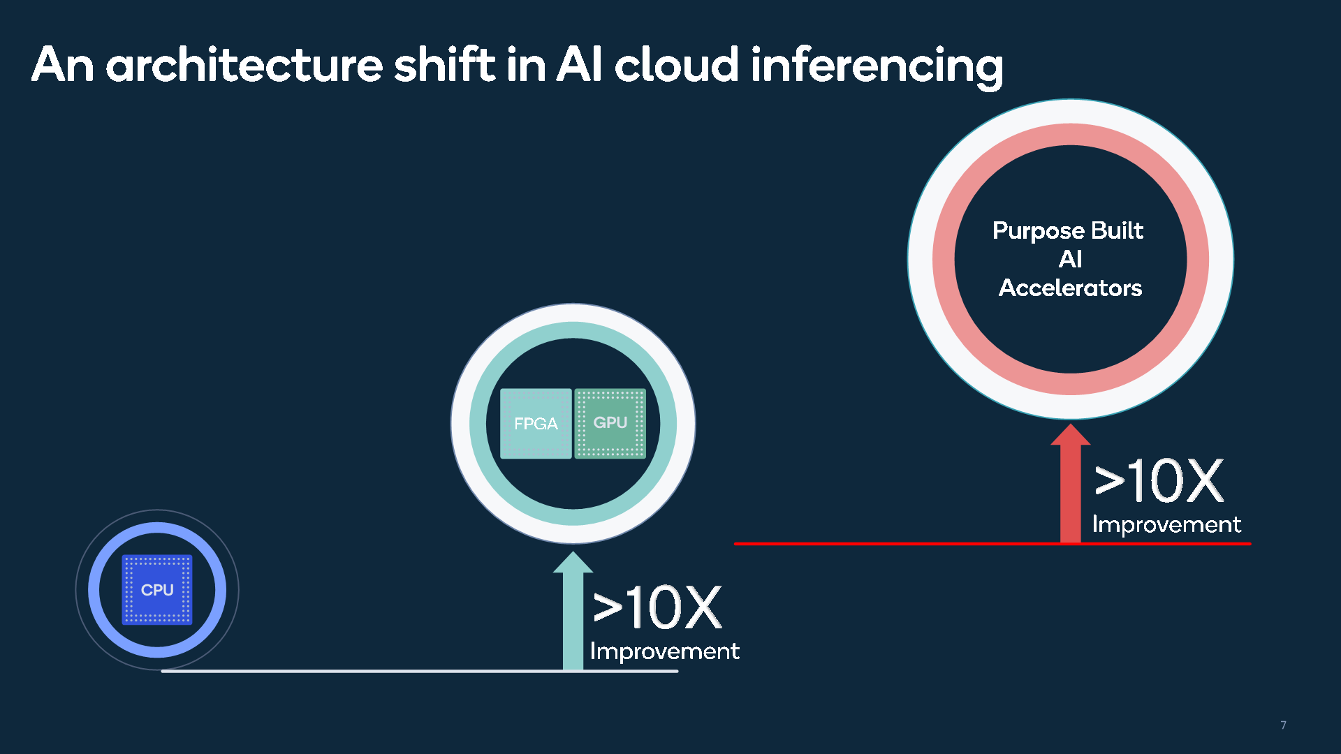
The big advantage of a dedicated AI design over current general-purpose computing hardware such as CPUs or even FPGAs or GPUs is that dedicated purpose-built hardware is able to achieve both higher performance and much higher power efficiency targets that are otherwise out of reach of “traditional” platforms.
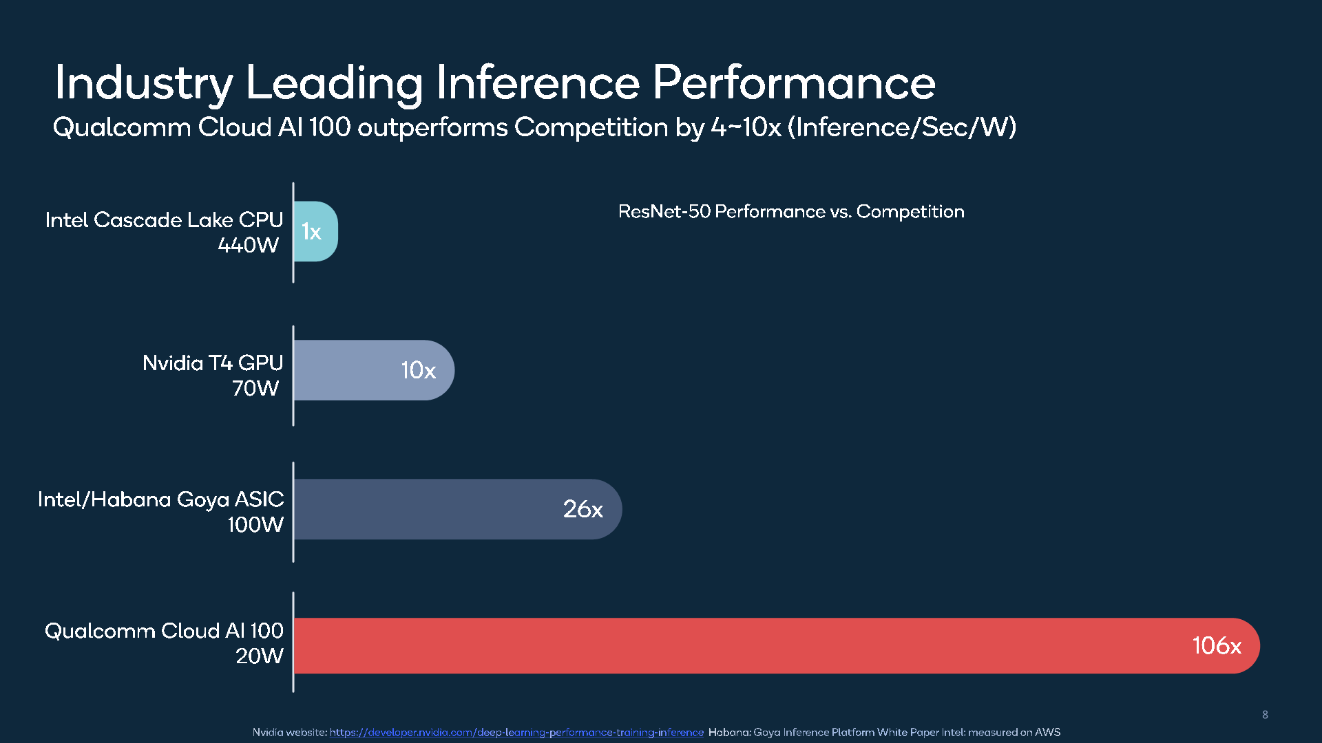
In terms of performance figures, Qualcomm presented ResNet-50 inference per second per watt figures against the currently most commonly deployed industry solutions, including Intel’s Goya inference accelerator or Nvidia’s inference targeted T4 accelerator which is based on a cut-down TU104 GPU die.
The Cloud AI 100 is said to achieve significant leaps in terms of performance/W over its competition, although we have to note that this chart does mix up quite a lot of form-factors as well as power targets as well as absolute performance targets, not being an apples-to-apples comparison.
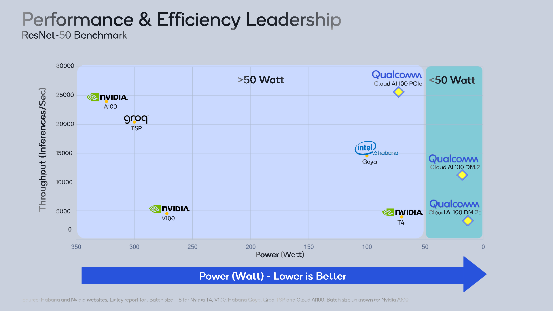
Qualcomm presents the dater in another performance/power chart in which we see a relatively fairer comparison. The most interesting performance claim here is that within the 75W PCIe form-factor, the company claims it’s able to beat even Nvidia’s latest 250W A100 accelerator based on the newest Ampere architecture. Similarly, it’s claiming double the performance of the Goya accelerator at 25% less power.
These performance claims are quite incredible, and that can be explained by the fact that the workload being tested here puts Qualcomm’s architecture in the best possible light. A little more context can be derived from the hardware specification disclosures:
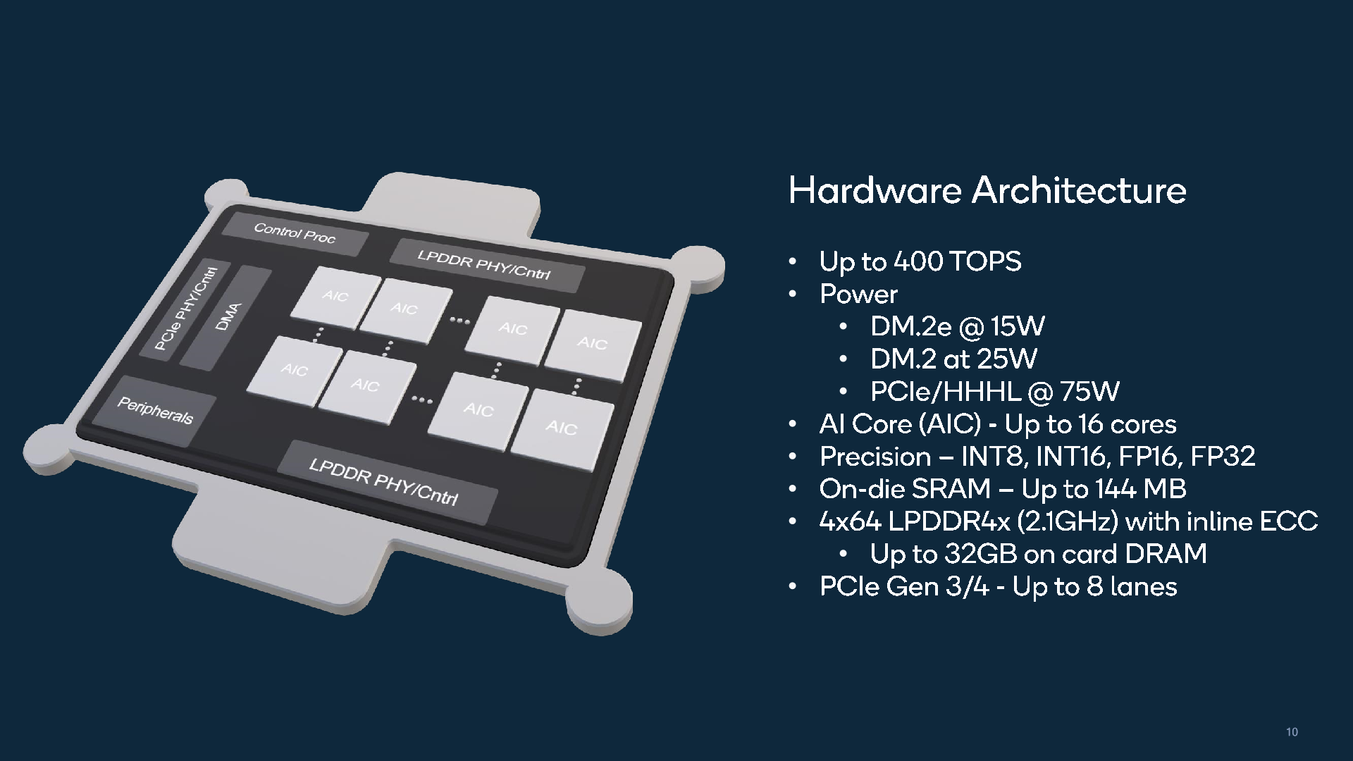
The chip consists of 16 “AI Cores” or AICs, collectively achieving up to 400TOPs of INT8 inference MAC throughput. The chip’s memory subsystem is backed by 4 64-bit LPDDR4X memory controllers running at 2100MHz (LPDDR4X-4200), each of the controllers running 4x 16-bit channels, which would amount to a total system bandwidth of 134GB/s.
For those familiar with the current AI accelerator designs, this bandwidth figure sounds extremely anaemic when put into context against competing design capabilities such as that of the A100 or the Goya accelerator which sport HBM2 memory and bandwidth capabilities of up to 1-1.6TB/s. What Qualcomm does to balance this out is to employ a massive 144MB of on-chip SRAM cache to keep as much memory traffic as possible on-chip.
Qualcomm admits that the architecture will perform differently under workloads whose kernels exceed the on-chip memory footprint, but this was a deliberate design balance that the company had agreed to make with its customers which have specific target workloads needs and requirements. Qualcomm expects that for larger kernels, the workloads will be scale-out across multiple Cloud AI 100 accelerators.
So, while Qualcomm’s performance figures in these specific ResNet-50 look fantastic, it might not paint the whole picture over a wider range of workloads. When asked when we should expect a wider range of benchmark result such as MLPerf submissions, the team did say that they have some sub-tests running internally, however the current short-term software engineering resources are focused on satisfying customer needs and optimising those workloads. Over time, we’ll see wider software support and eventual MLPerf performance figures.
When asked about how the company is achieving such a broad dynamic range (15W to 75W) in terms of power targets with a single silicon design, the company explains that they are tuning the frequency/voltage curves as well as modulating the number of active AI Cores in the design. Imagine that the full 400TOPS 75W design to contain a fully working chip at higher frequencies, while the 15W design might have units disabled as well as running at a lower frequency. The 7nm process node also greatly helps with keeping power consumption low.
The PCIe interface supports the latest 4.0 standard with 8x lanes.
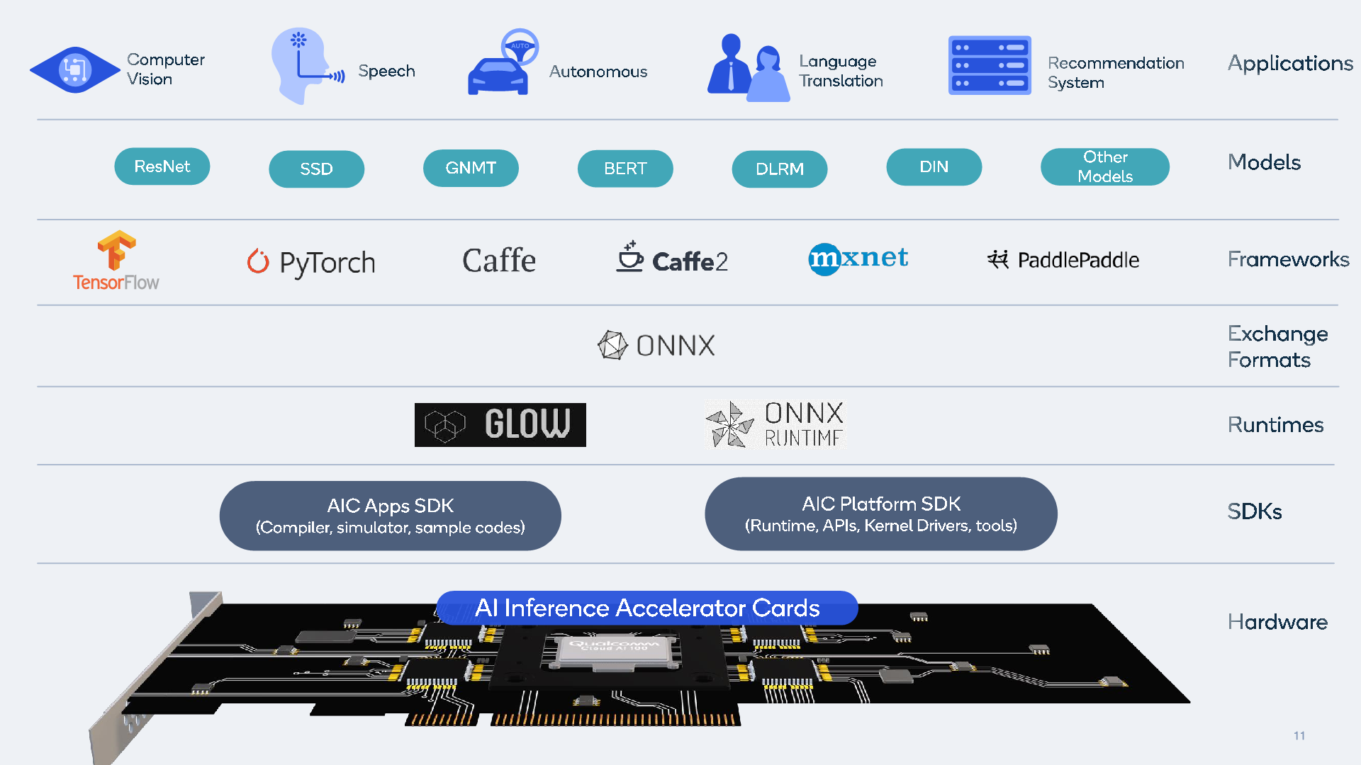
Precision-wise, the architecture supports INT8, INT16 as well as both FP16 and FP32 precisions which should give it plenty of flexibility in terms of supported models. Qualcomm also provides a set of SDKs for support of a set of industry standard runtimes, exchange formats and frameworks.
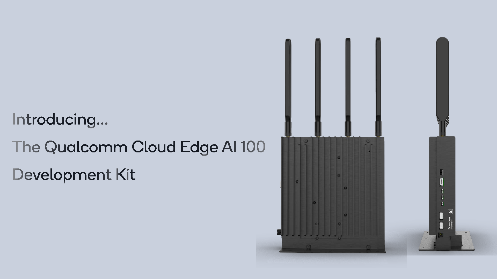
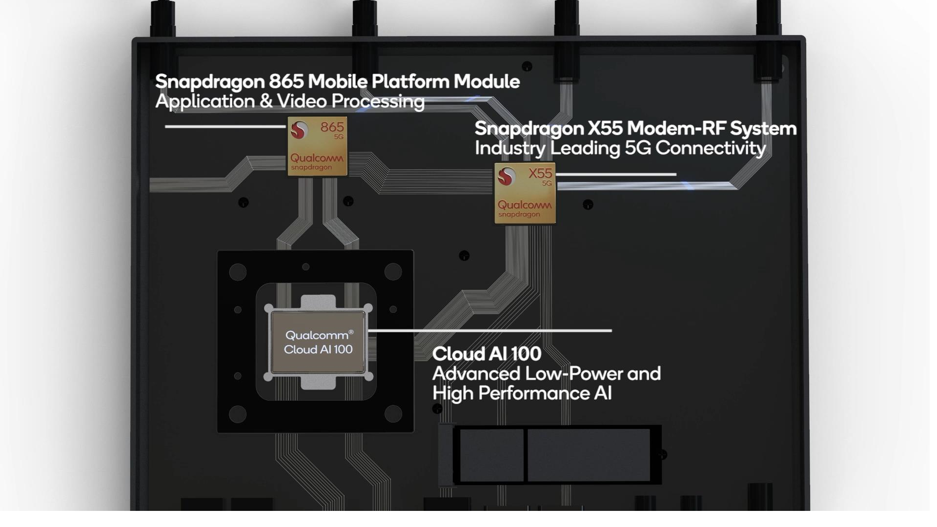
Qualcomm is currently sampling the Cloud AI 100 to customers with targeted deployments being primarily edge-inference workloads in the industry and commerce. In order to kick-start the ecosystem and enable software development, Qualcomm is also introducing the new Cloud Edge AI 100 Development Kit which consist of an integrated small form-factor computing device housing the Cloud AI 100 accelerator, a Snapdragon 865 system SoC and a X55 5G-modem for cellular connectivity.
Commercial shipments to customers are expected in the first half of 2021.


14 Comments
View All Comments
Yojimbo - Wednesday, September 16, 2020 - link
Firstly, it's not good that they are talking about inference and never once mention latency. Secondly, throughput is fast on ResNet-50 because ResNet-50 is small and fits in its cache. But ResNet-50 is also much smaller than what most data centers are running inference on these days, to my understanding. Architectures like this definitely need MLPerf scores to confirm their claims, much like Graphcore, which claims it can stream larger networks effectively from DDR memory but still has no MLPerf results published. This thing, similarly, will be relying on DDR memory for anything that doesn't fit in its internal cache.frbeckenbauer - Wednesday, September 16, 2020 - link
The huge on-chip SRAM cache is what's being rumored for the "big navi" GPUs, interestingfangdahai - Wednesday, September 16, 2020 - link
>>Precision-wise, the architecture supports INT8, INT16 as well as both FP16 and FP32I guess 400TOPS is based on INT8. How about FP32? 50TOPS?
ChrisGX - Friday, September 25, 2020 - link
I am sceptical that Qualcomm will be able to succeed with a product like this. While the TOPs thing is probably a distraction when what we need is benchmarking based on well chosen workloads running on AI Infererence Accelerators, there will still be the inevitable comparisons using those TOPs numbers. And, things take on a strange look when we go down that path:Qualcomm claims 400TOPs at 75W for the Cloud AI 100 > 5.3TOPs/W
Gyrfalcon Technology claims 16.8 TOPs at 700mW for the Lightspeeur 2803S > 24TOPs/W
Perceive claim very high performance at 20mW for the Ergo edge inference processor > 55 TOPs/W
Imec and GLOBALFOUNDRIES claim orders of magnitude higher performance for their Analog Inference Accelerator (with the ambition to evolve the technology even further) > 2,900 TOPs/W (evolving towards 10,000 TOPS/W)
While the accelerators listed here aren't directly comparable to Qualcomm's Cloud AI 100 (for Cloud Edge data centres) I don't see the job of putting a compelling case for one technology or another to potential users as being an easy one while ever the long term viability of the technologies on offer and the soundness of investment in those technologies is in question.