Hot Chips 2021 Live Blog: CPUs (Alder Lake, Zen3, IBM Z, Sapphire Rapids)
by Dr. Ian Cutress on August 23, 2021 10:30 AM EST- Posted in
- CPUs
- AMD
- Intel
- Xeon
- Trade Shows
- SoCs
- IBM
- DDR5
- Zen 3
- IBM Z
- Sapphire Rapids
- Alder Lake
- Hot Chips 33
- V-Cache
11:40AM EDT - Welcome to Hot Chips! This is the annual conference all about the latest, greatest, and upcoming big silicon that gets us all excited. Stay tuned during Monday and Tuesday for our regular AnandTech Live Blogs. Today we start at 8:45am PT, so set your watches and notifications to return back here! The first set of talks is all about CPUs: Intel Alder Lake, AMD Zen 3, IBM Z, and Intel Sapphire Rapids.
11:45AM EDT - The stream should be starting momentarily
11:45AM EDT - It usually starts with 15 minutes of pre-show info to begin

11:47AM EDT - Here we go
11:48AM EDT - Apparently some attendees are having issues with too many from the same company on the same VPN
11:49AM EDT - There's a slack channel for all attendees
11:49AM EDT - Behind the scenes
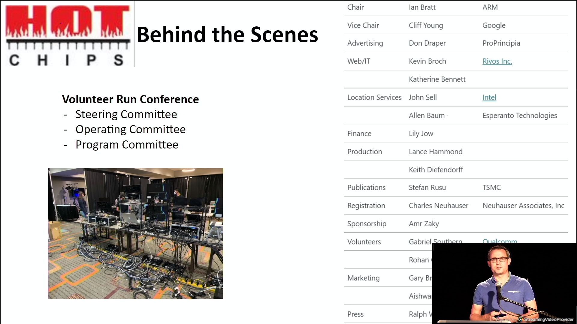

11:51AM EDT - Lots of members on the committees
11:51AM EDT - Selecting the best talks
11:51AM EDT - These people identify keynote speakers, solicit papers for talks
11:52AM EDT - Tutorials were yesterday
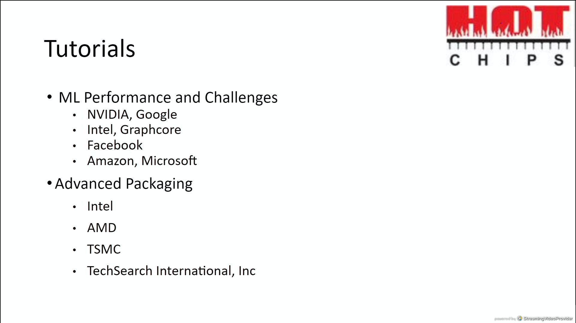
11:54AM EDT - Three keynotes
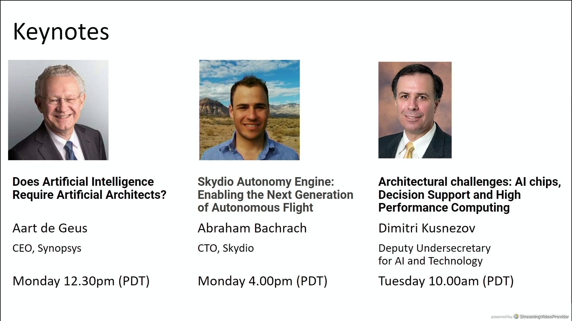
11:55AM EDT - Synopsys is on AI in EDA
11:55AM EDT - Skydio on autonomous flight
11:55AM EDT - DoE on AI Chips and challenges
11:56AM EDT - 'Chips enabling Chips'
11:57AM EDT - For those attending
11:57AM EDT - Posters as part of the conference as well
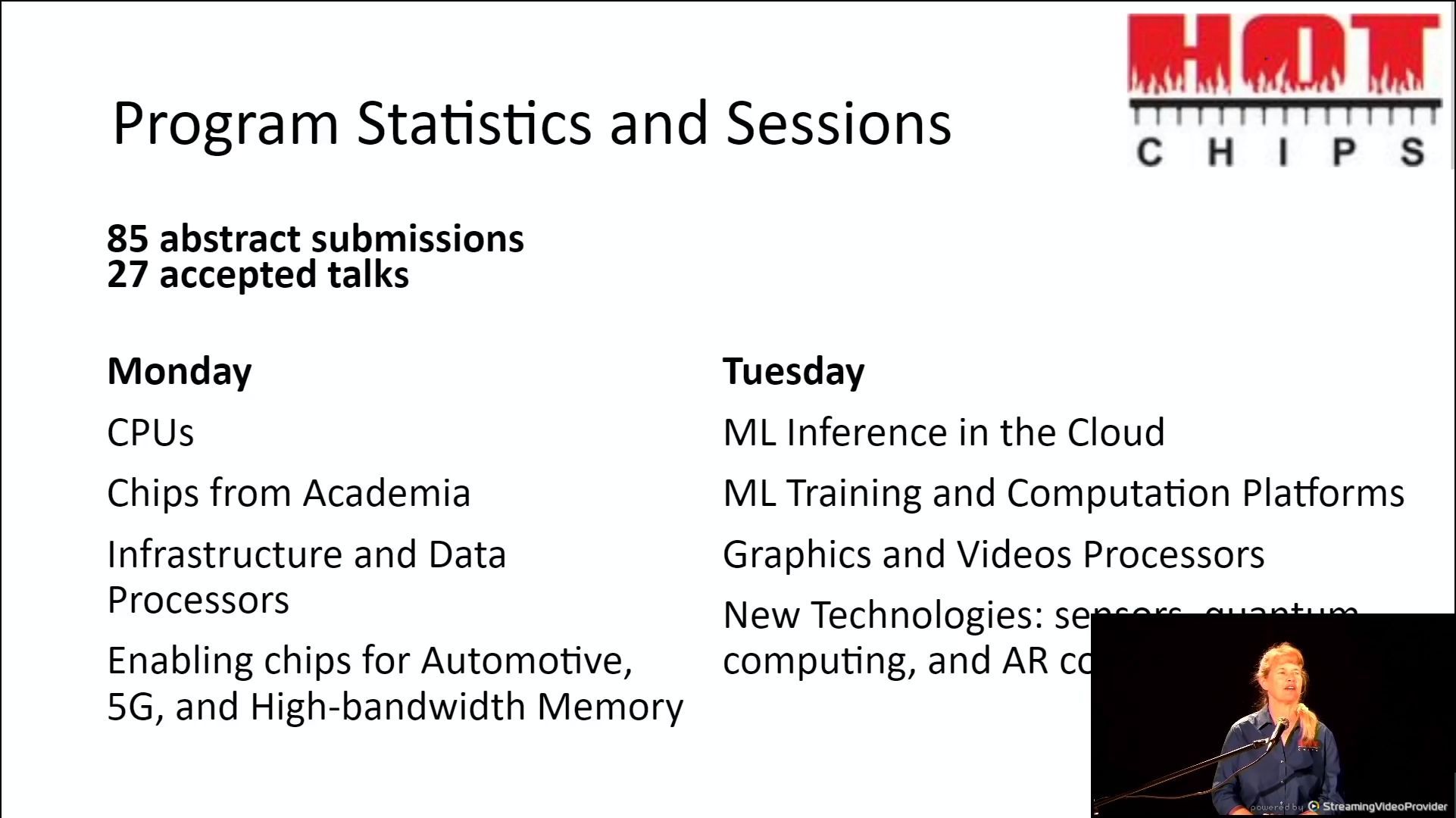
11:58AM EDT - First session is CPUs, about to start
11:59AM EDT - 'State of the art CPUs'
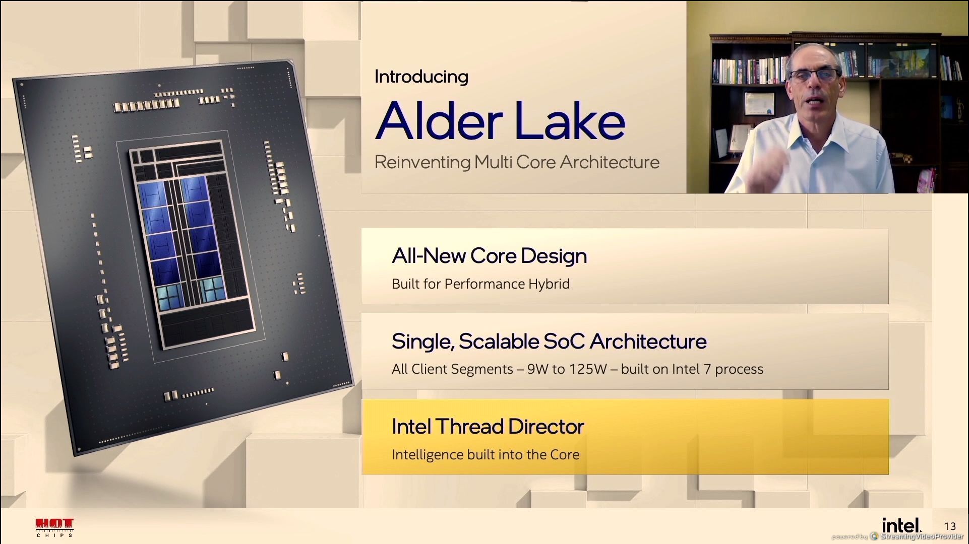
11:59AM EDT - Efi Rotem for Intel on Alder Lake
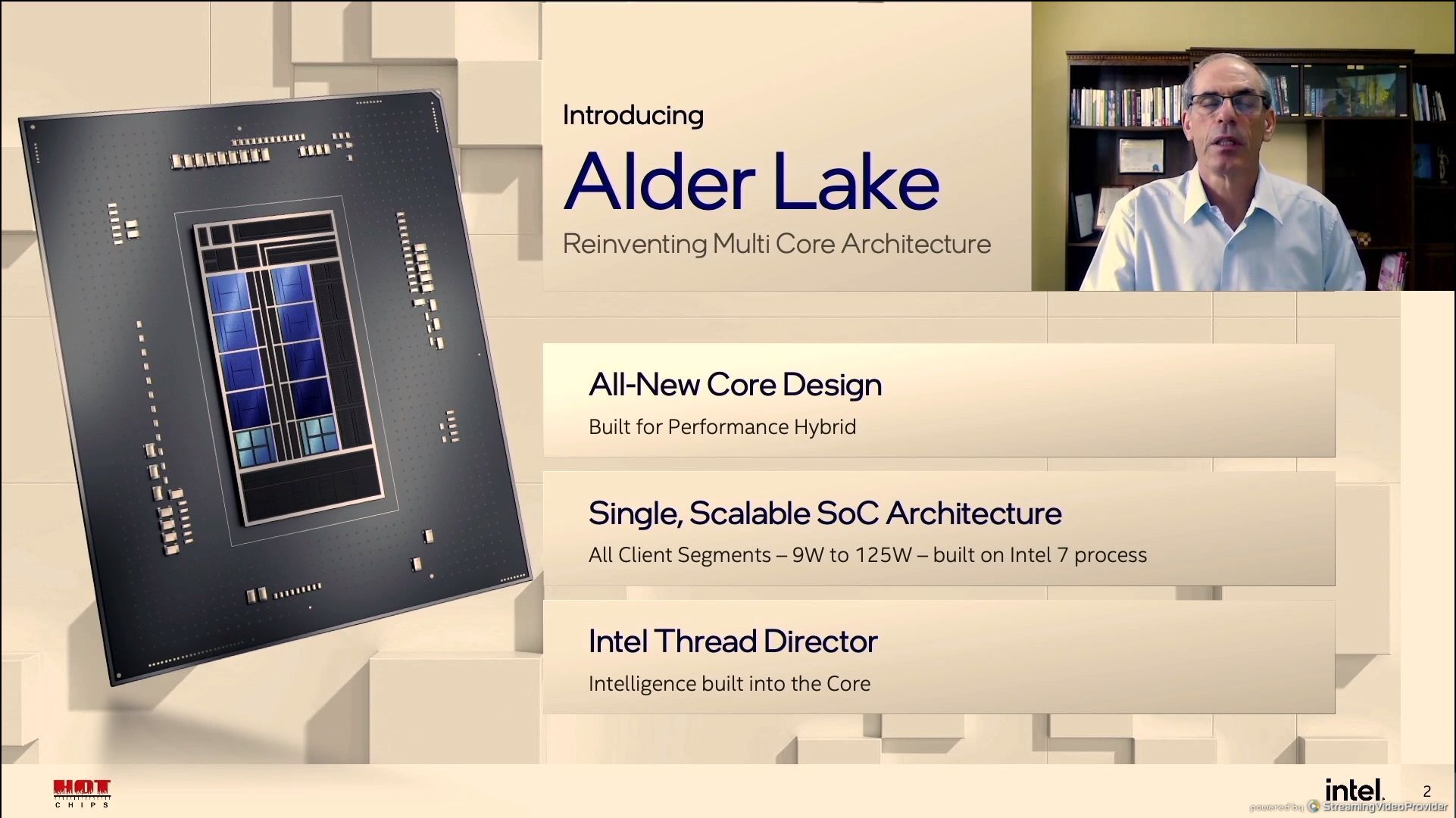
12:00PM EDT - The why and how of Alder Lake
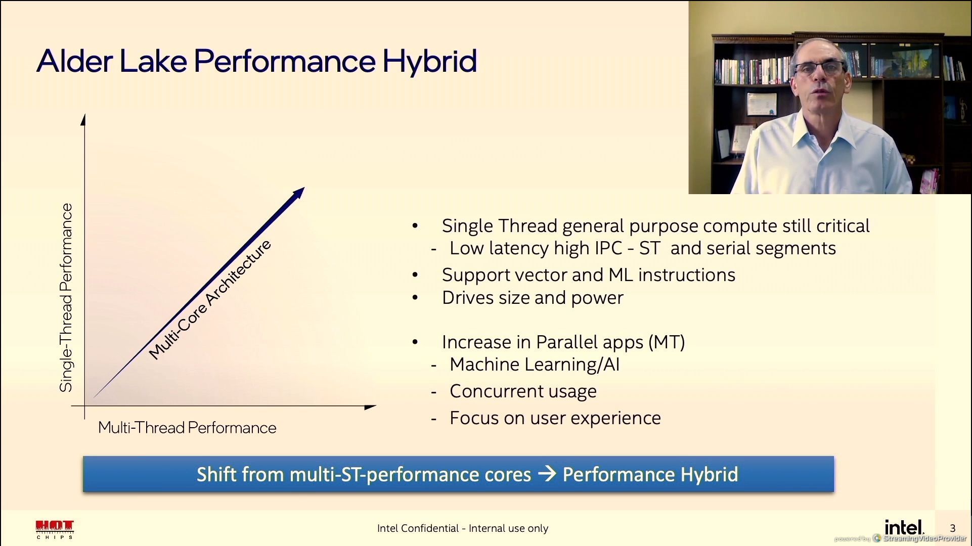
12:00PM EDT - Most apps are Single or lightly MT
12:01PM EDT - Increase in support of ML
12:01PM EDT - Working on smarter structures and new instructions for ML
12:01PM EDT - Duplicating multicore
12:02PM EDT - Moores Law and Dennard Scaling
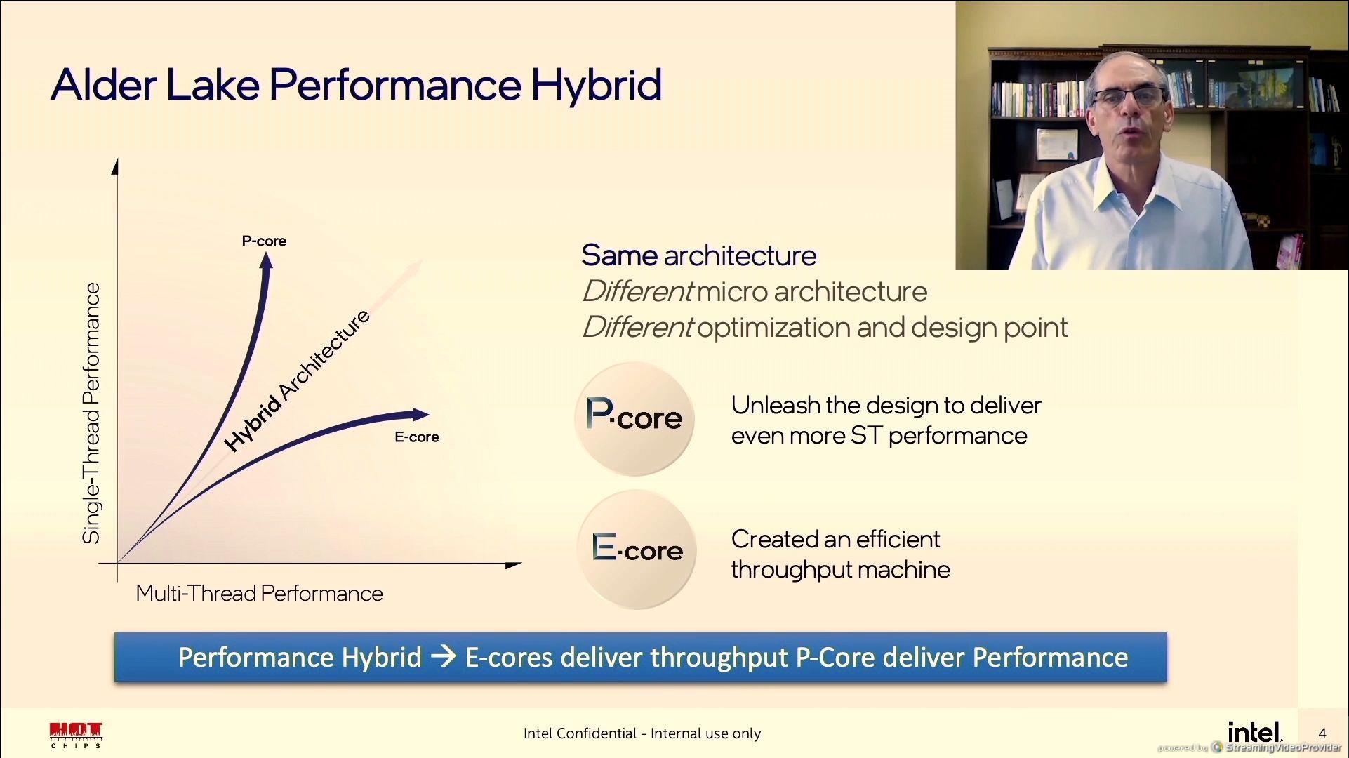
12:02PM EDT - Same arch, different uArch, different opimization point
12:03PM EDT - This is what we saw in the Alder Lake part of the Architecture Day
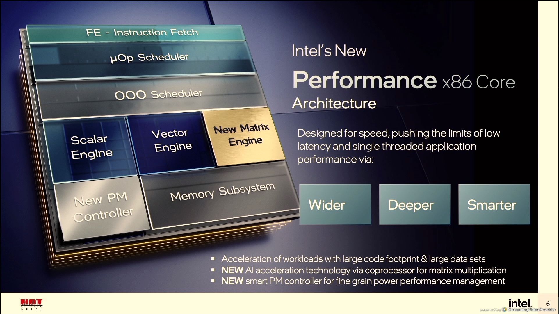
12:03PM EDT - P-Core and E-Core
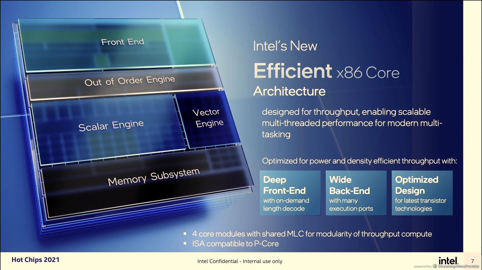
12:04PM EDT - E-core has shared L2
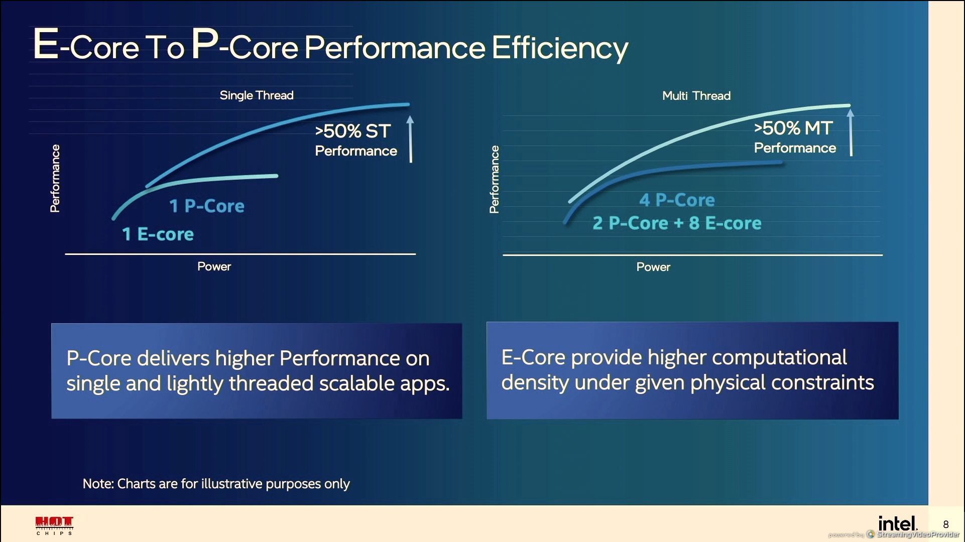
12:04PM EDT - P-core is +50% ST performance over the E-core
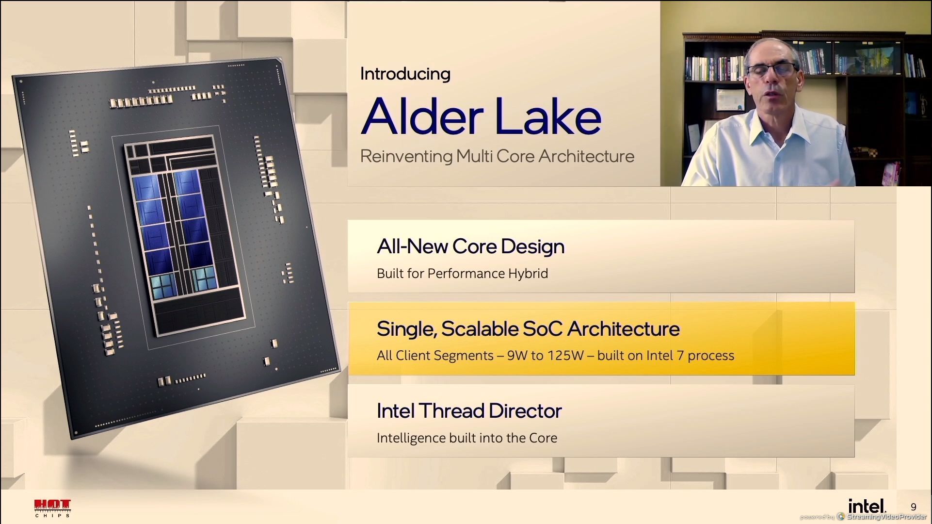
12:05PM EDT - Scalable SoC architecture
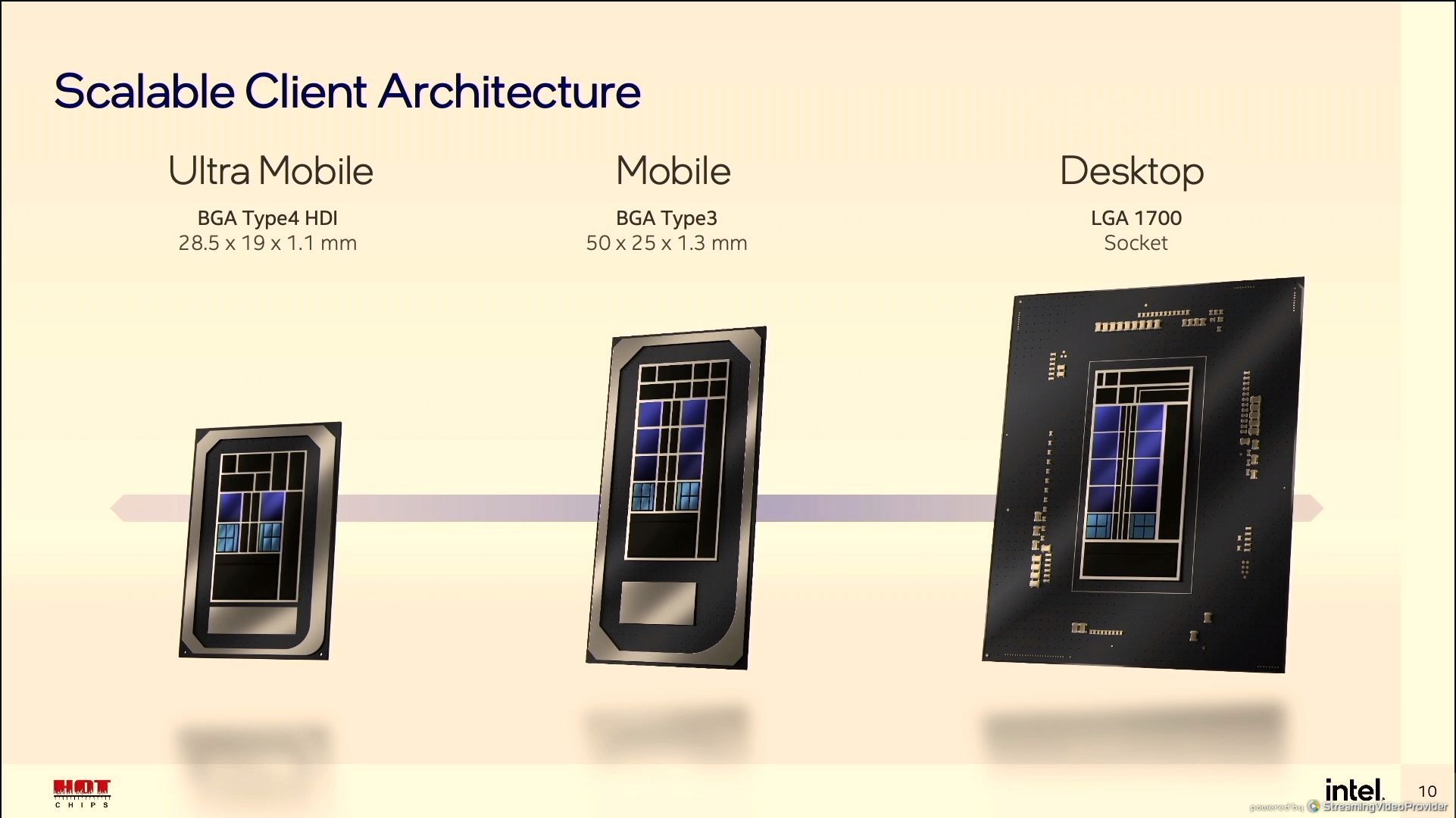
12:05PM EDT - UP3/UP4 for mobile, Desktop
12:05PM EDT - 2+8, 6+8 and 8+8 for P-core + E-core
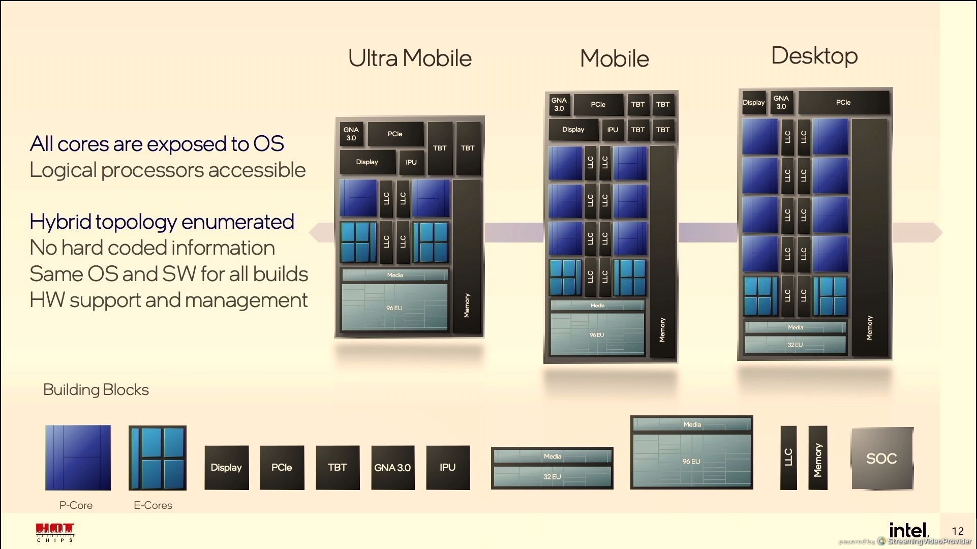
12:06PM EDT - modular design
12:06PM EDT - mix and match for future products
12:06PM EDT - 96 EUs on mobile, 32 EUs on desktop
12:07PM EDT - Only mobile will get native Thunderbolt
12:08PM EDT - Smartness is built into the hardware
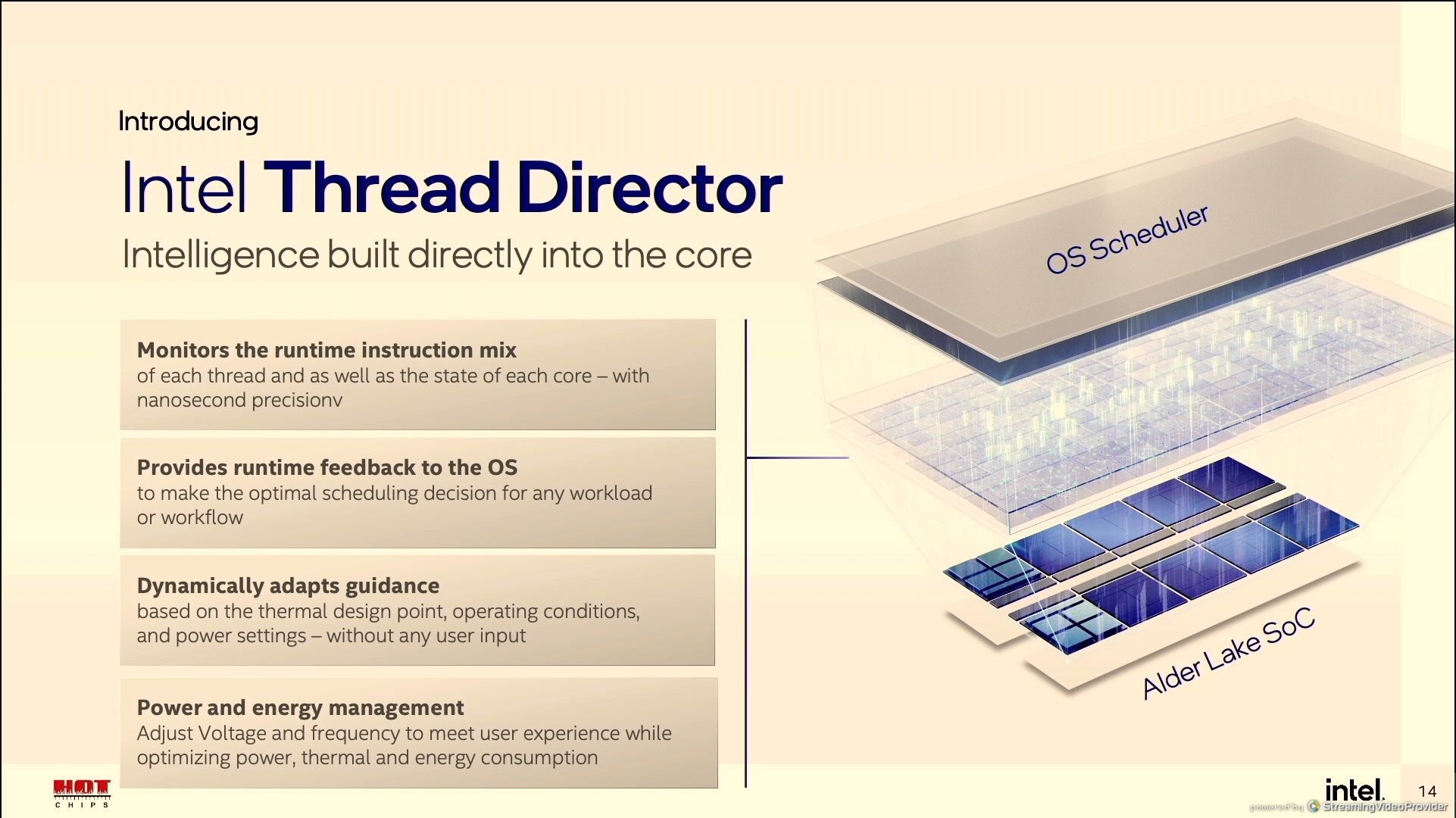
12:08PM EDT - Thread Director is mostly for Window 11
12:09PM EDT - Onboard microcontroller

12:10PM EDT - Thread Director will predict the class of workload and bucket it the classes for the OS scheduler on the oder of 30 microseconds
12:10PM EDT - Core-to-Core IPC is the main metric
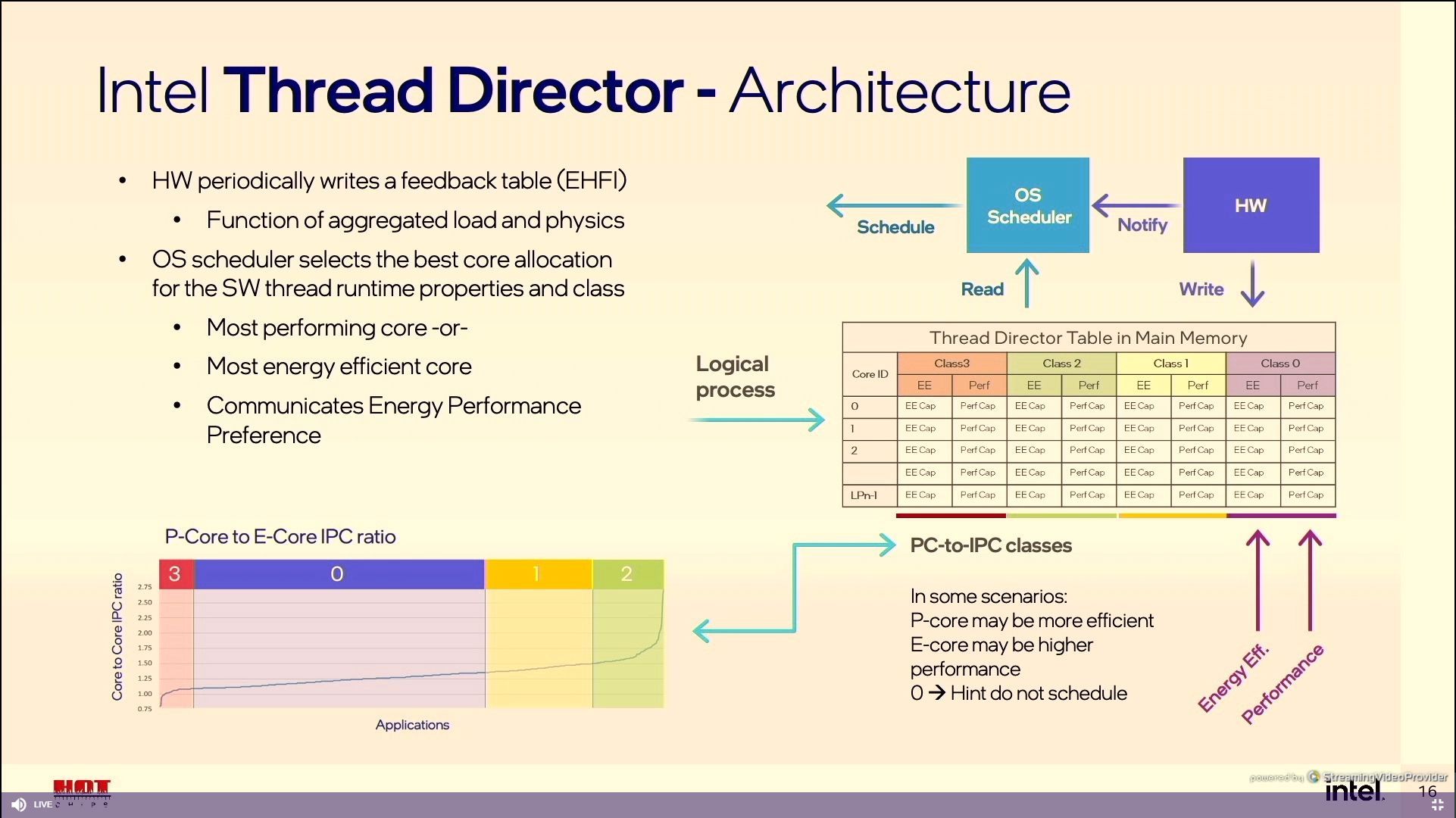
12:11PM EDT - Intel EHFI
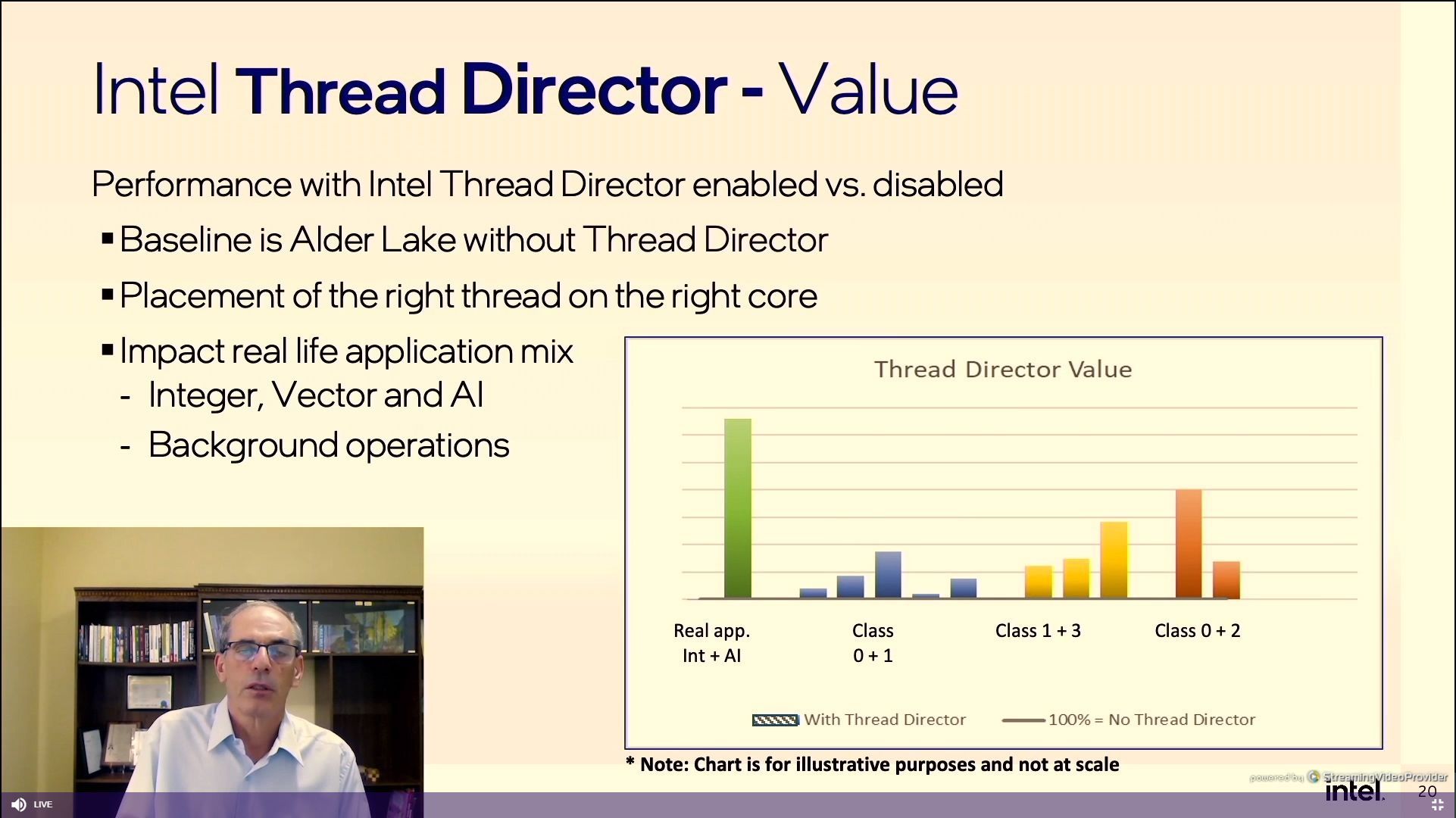
12:12PM EDT - This is more detail about Thread Director
12:12PM EDT - So every processor gets a section in the table, and it has a value for Perf and Efficiency, and workload is compared
12:14PM EDT - Sometimes it makes sense to coalesce a software thread to fewer cores, or one type of core
12:14PM EDT - Thread Director Table updated less often than thread classification
12:14PM EDT - OS has idea of priority of thread
12:15PM EDT - OS scheduler is final arbiter
12:15PM EDT - Table is topology agnostic
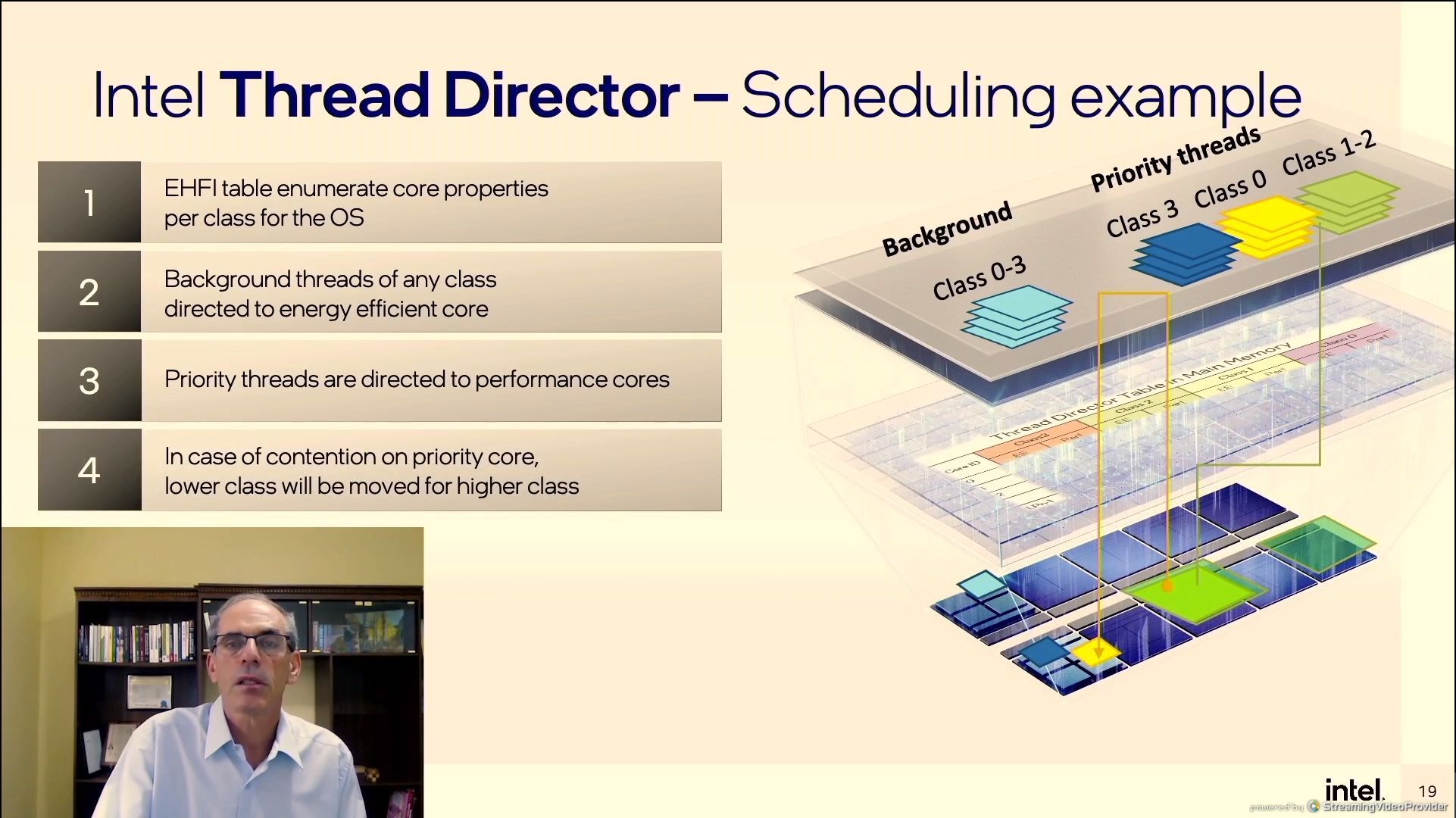
12:17PM EDT - Here's a scheduling example
12:18PM EDT - Helps with asymmetry between the threads
12:19PM EDT - All AI workloads go to P-Cores over anything else
12:19PM EDT - AVX + VNNI / INT8 get highest priority over anything
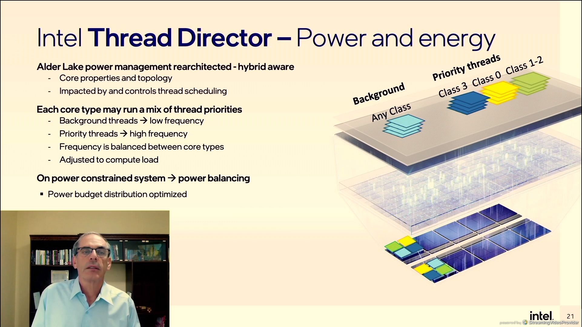
12:21PM EDT - EPP - Energy Performance Preference also takes a role in input to the scheduler
12:21PM EDT - For power constrained systems
12:21PM EDT - higher priority gets higher voltage and frequency regardless of P-core and E-core
12:22PM EDT - optimal P/V point is a function of phyiscal properties (thermal, binning)
12:22PM EDT - Q&A time
12:23PM EDT - Q: Security of side channel attacks with Thread Director A: No security effect, only performance
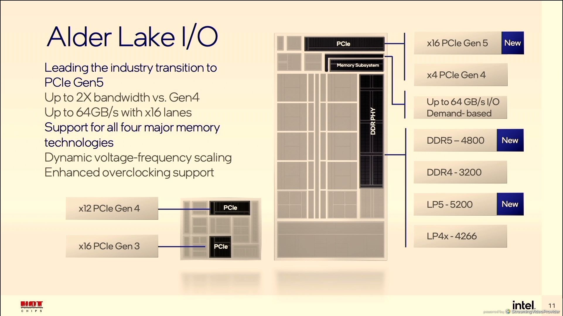
12:24PM EDT - Q; Die photo, PCIe - how many PCIe 5/4/3 lanes? A: As shown, slide 11, 16x PCIe 5, 4x lanes of PCIe 4, Desktop has PCH
12:25PM EDT - Q: TDT for Linux, when? A: First enabling was Windows 11, work with Linux for time - it is coming, which version and build will be published later
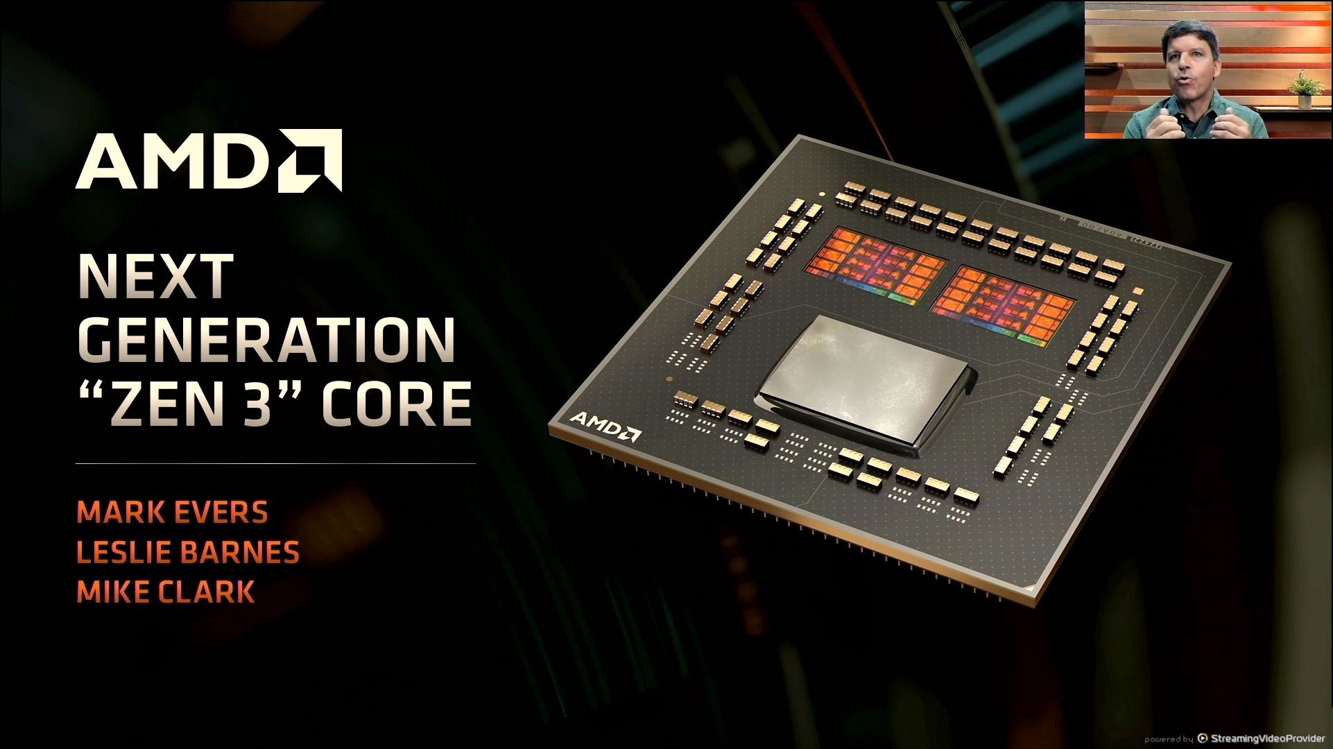
12:25PM EDT - Now AMD Zen 3 talk
12:26PM EDT - Mark Evers from AMD
12:26PM EDT - The Zen Journey from 2017
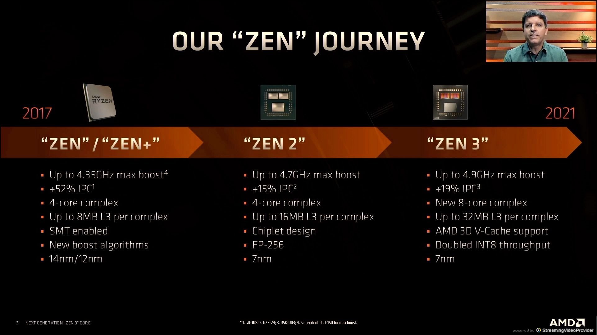
12:27PM EDT - New era in the market for AMD
12:27PM EDT - Zen3 says AMD 3D Cache support
12:27PM EDT - Exceeding Industry Trends
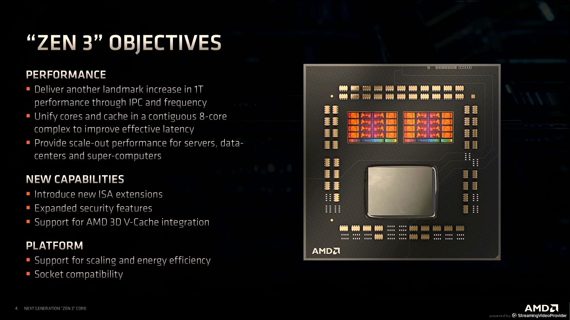
12:28PM EDT - Scale-out for servers and supercomptuers
12:28PM EDT - Socket compatibility for past products
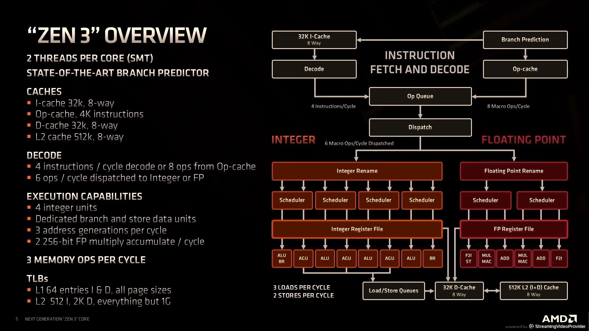
12:29PM EDT - 4k op cache
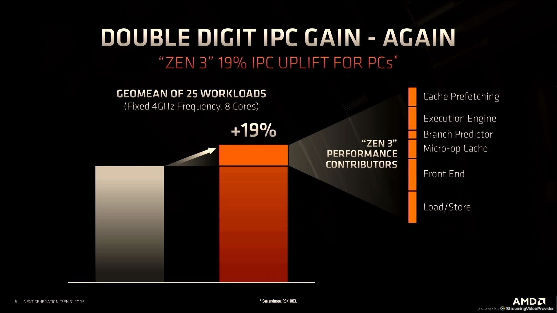
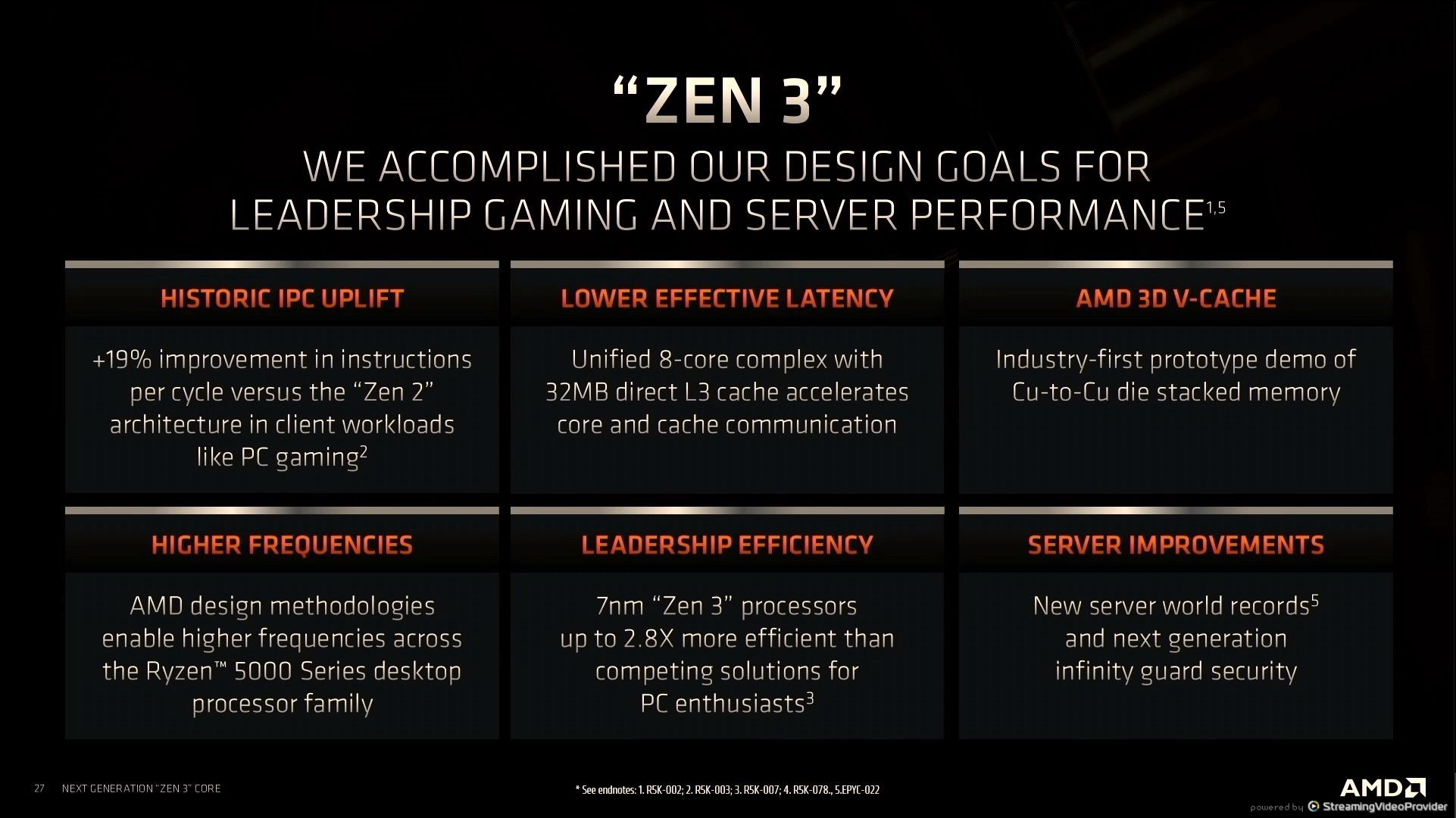
12:30PM EDT - +19% IPC gains, which we verified at launch
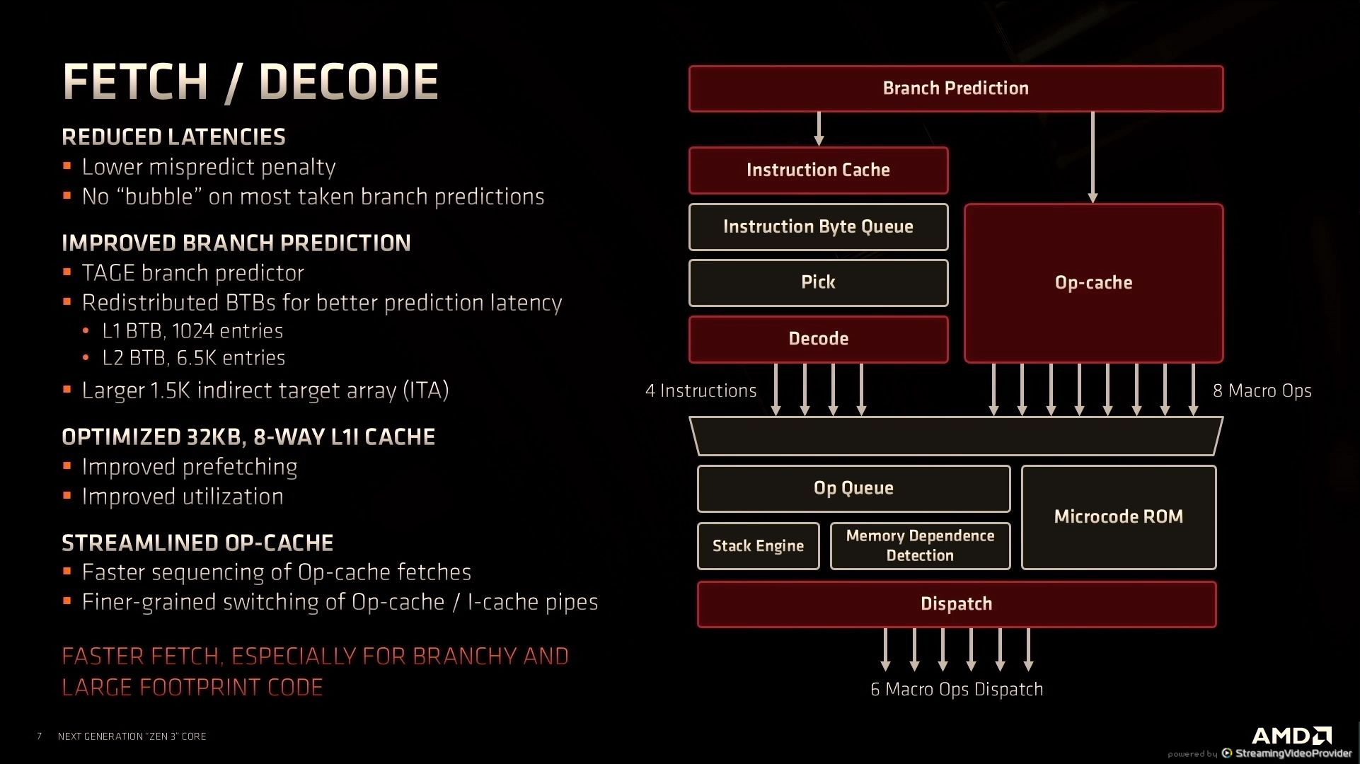
12:31PM EDT - Large chunk of performance gain from the front end fetch/decode
12:31PM EDT - reduced bubble cycle latency
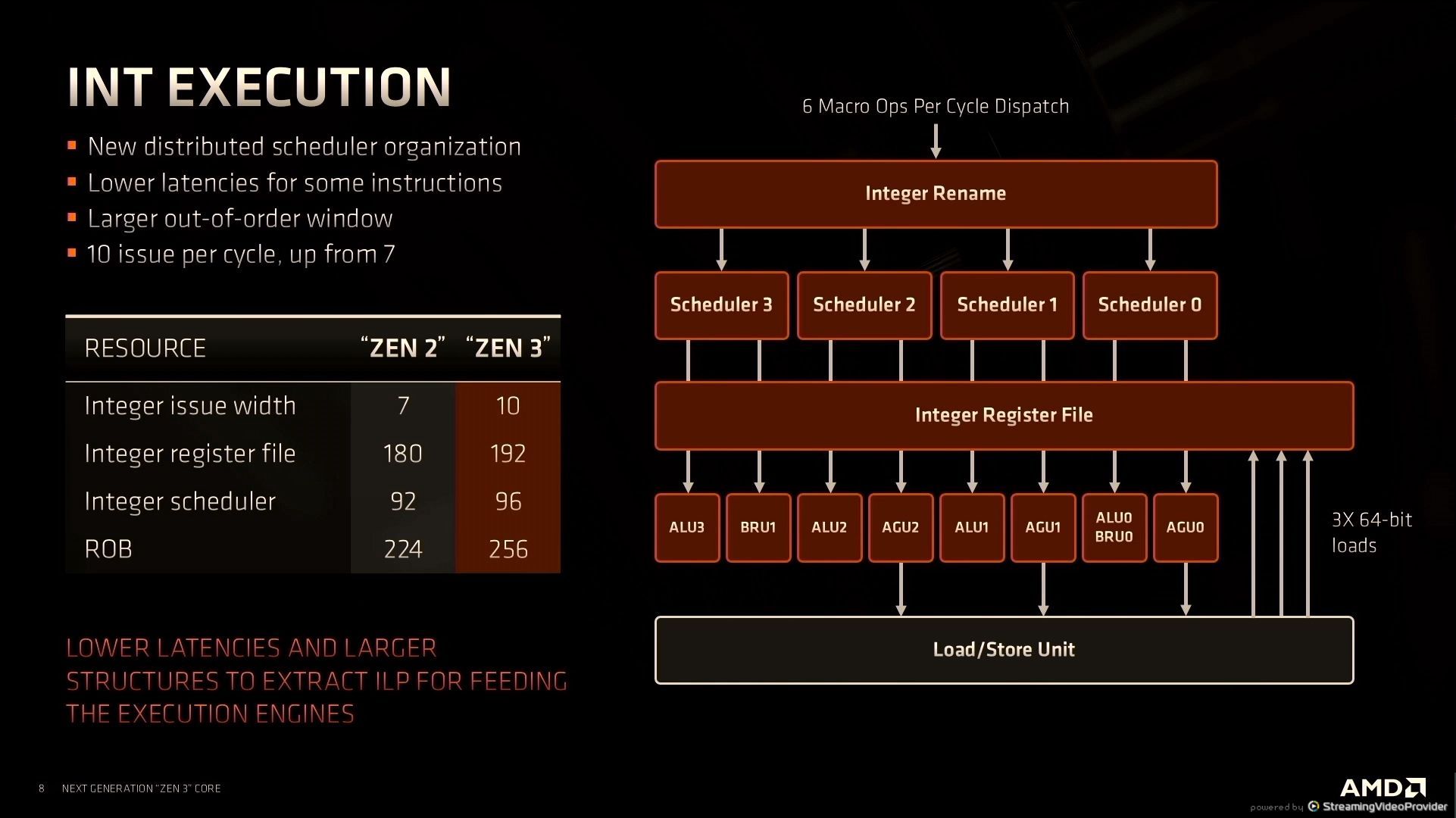
12:32PM EDT - supporting wider execution
12:32PM EDT - lower latencies for some instructions
12:33PM EDT - 10 issue per cycle up from 7
12:33PM EDT - More execution bandwidth ILP extraction
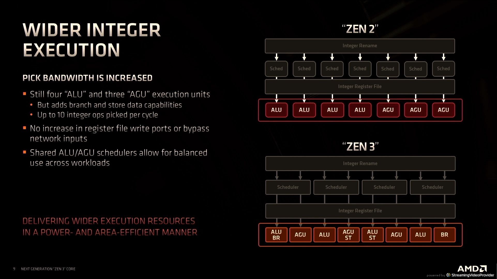
12:33PM EDT - Disaggregated the ALUs rather than just add more
12:34PM EDT - Without any additional increase in register file ports
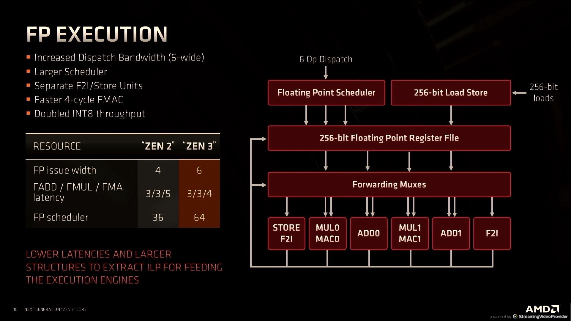
12:34PM EDT - larger 6-wide FP unit
12:34PM EDT - Faster 4-cycle FMAC
12:34PM EDT - Reduced FMA latency
12:34PM EDT - Doubled INT8 throughput

12:35PM EDT - larger load-store
12:35PM EDT - L2 DTLB has 6 page walkers
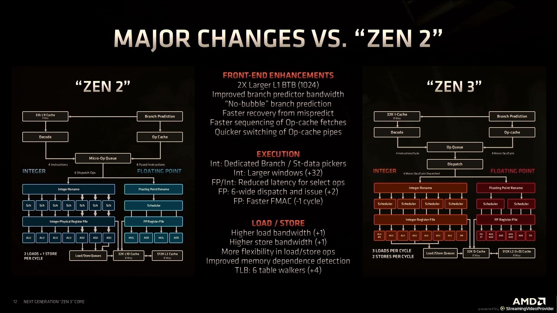
12:36PM EDT - Changes from Zen2
12:36PM EDT - Removed bubble cycle with branch prediction
12:37PM EDT - Back on track faster when mispredict
12:37PM EDT - Quicker switching with I-cache overflow

12:38PM EDT - How AMD calculated IPC uplift

12:39PM EDT - Enterprise security additions
12:39PM EDT - SEV, SEV-ES, SEV-SNP
12:39PM EDT - SNP is the new feature for Zen 3
12:40PM EDT - Eliminates page table attack vectors through VMs/hypervisors
12:40PM EDT - No application modification needed
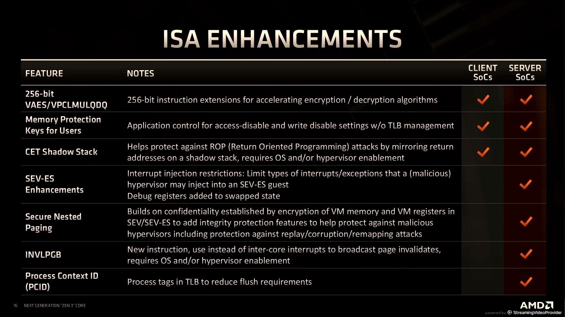
12:40PM EDT - New instruction support
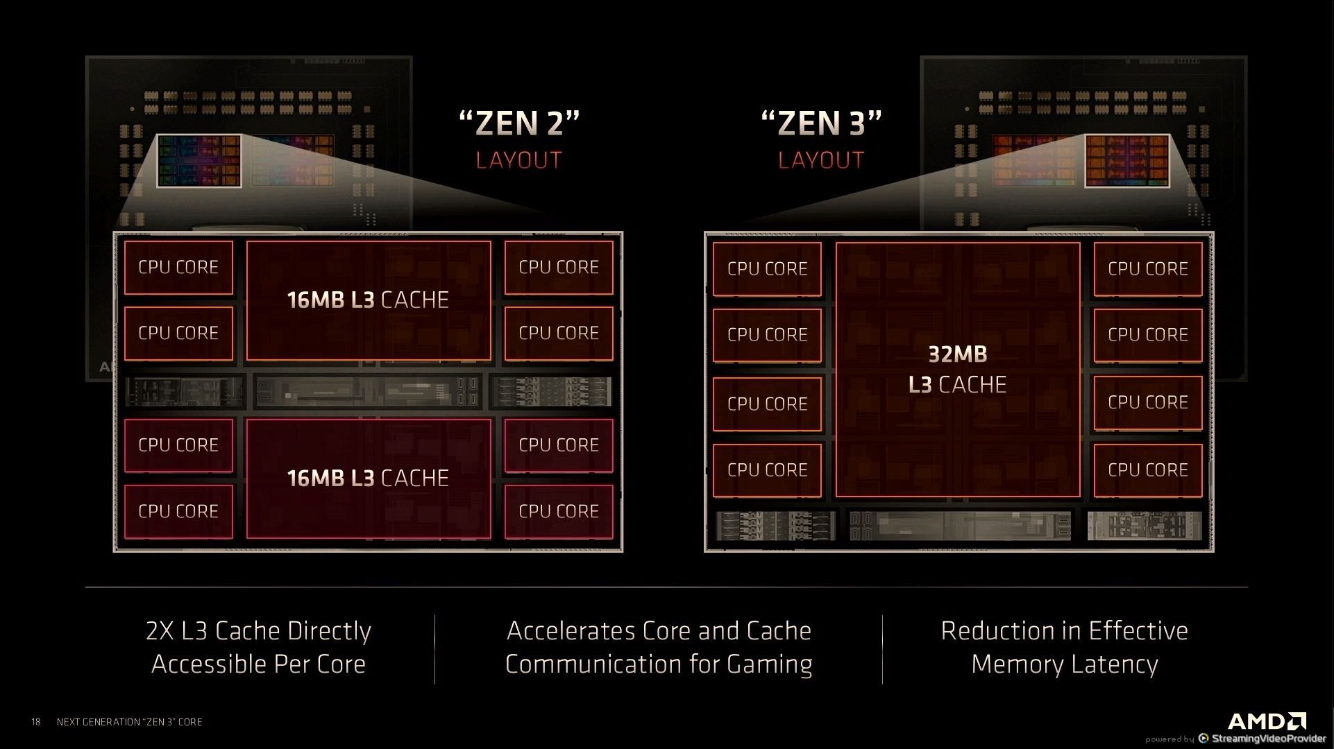
12:41PM EDT - Double L3 cache
12:42PM EDT - access from cores, better for gaming
12:42PM EDT - reduction in effective L3 memory latency
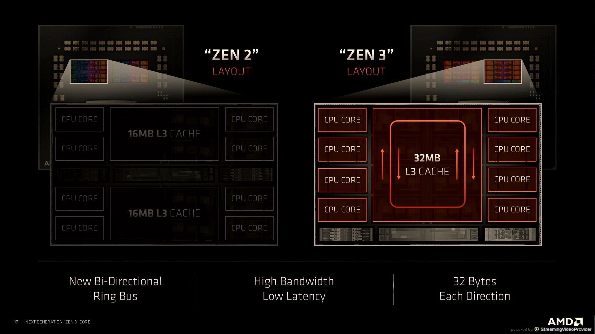
12:42PM EDT - 2x32B data channels in opposite directions
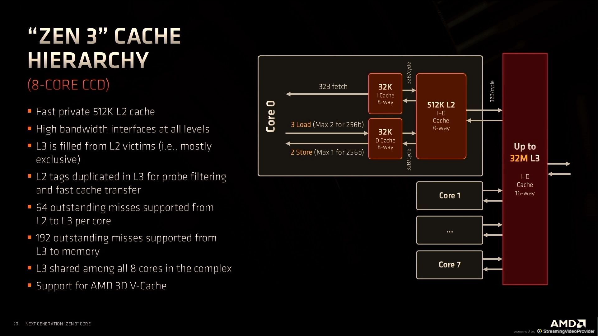
12:43PM EDT - L3 is an non-inclusive cache
12:43PM EDT - L2 tags in L3
12:43PM EDT - support 192 misses from L3 to memory
12:44PM EDT - Built in support for AMD V-Cache
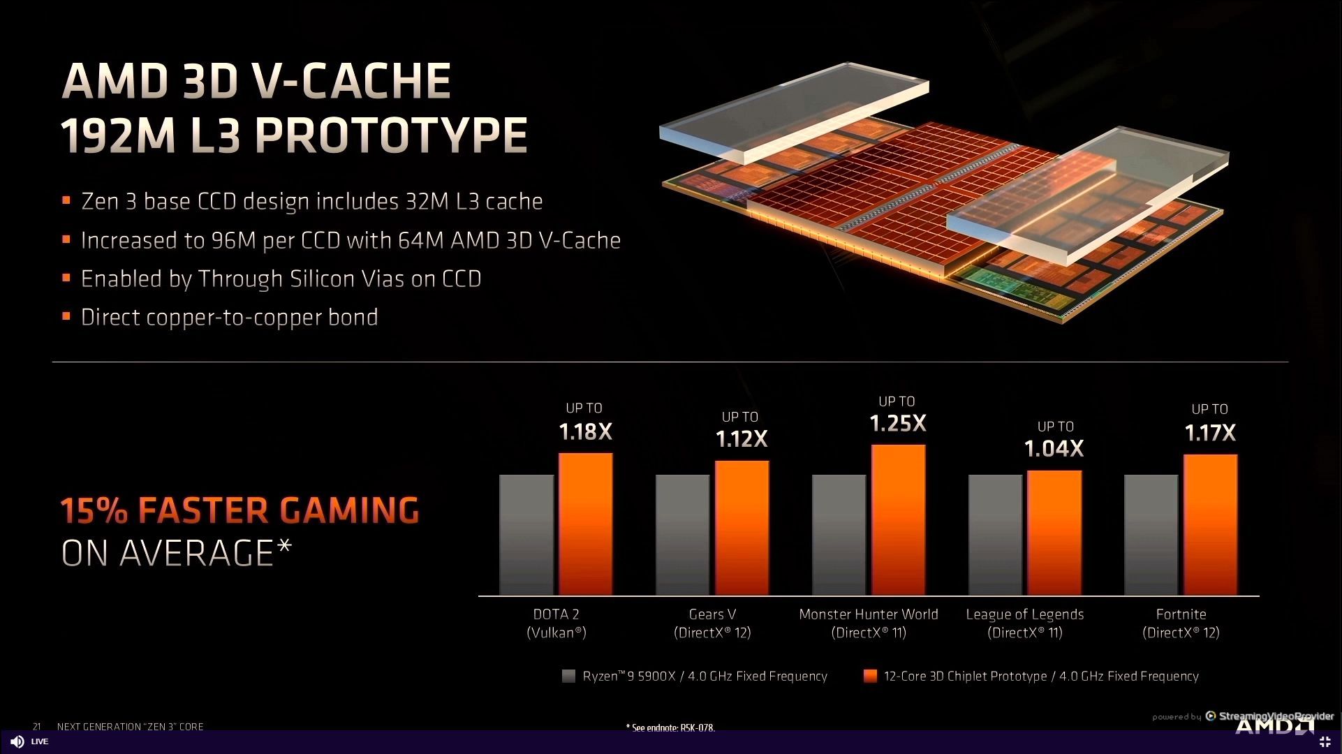
12:44PM EDT - Already demoed +64 MB L3
12:44PM EDT - +15% faster on gaming
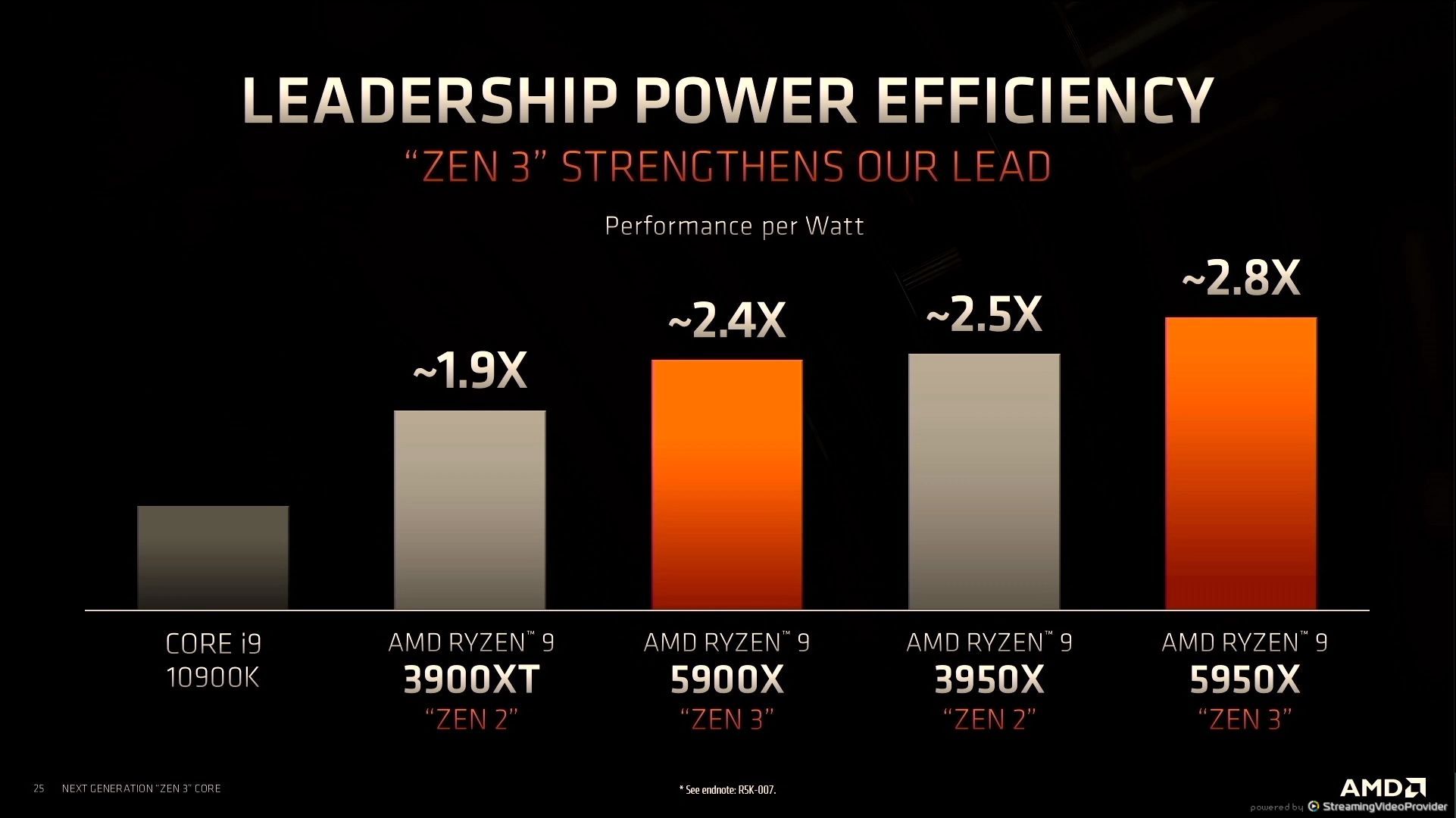
12:47PM EDT - Ryzen performance gains in the same TSMC 7nm
12:47PM EDT - All from uarch and physical design

12:47PM EDT - Gaming was a main target for Zen 3
12:48PM EDT - Performance that matters for the user
12:49PM EDT - Summing up
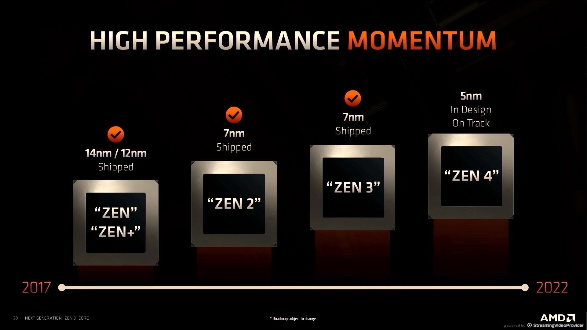
12:49PM EDT - Zen4 by end of 2022
12:49PM EDT - On track in TSMC N5
12:50PM EDT - Time for Q&A
12:51PM EDT - Q: V-Cache is applicable all the segments, all just for desktop/server A: Lot of different workloads, benefit from v-cache, Havenlt announced specific products with v-cache, but some workloads across segments that benefit
12:52PM EDT - Q: Primary motication for tripling table walkers A: some workloads with large DRAM access footprint with outstandling TLB misses. Lots of workloads won't need more than 2, but benefits a few pages, but a clever way to add more without excessive
12:54PM EDT - Q: Is the chiplet technology technology scalable? A: When it comes to the 3D Vcache - latency is not large. For chiplets of having CCDs and IODs, it can give you more flexibility than monolithic. Build best products with chiplets
12:55PM EDT - Next presentation is from IBM
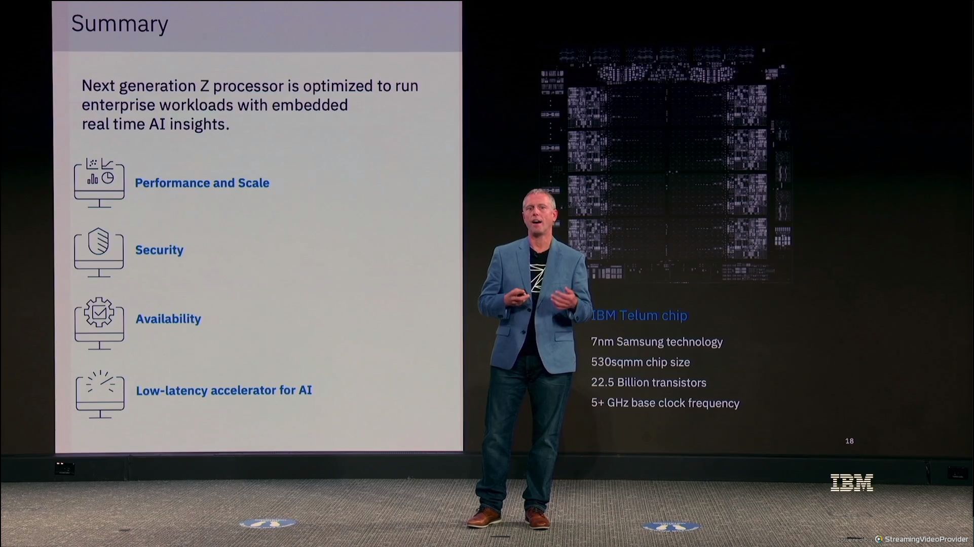
12:55PM EDT - IBM Telum Processor
12:55PM EDT - Optimized from AI
12:55PM EDT - Next Gen Z processor
12:55PM EDT - This would be IBM z16, but this one gets a name

12:56PM EDT - How often do you use a mainframe? Probably yes if you've used your credit card
12:57PM EDT - Chief Architect
12:57PM EDT - Starting with background on IBM z
12:57PM EDT - large part of IT infrastructure
12:58PM EDT - Even startups with NFTs
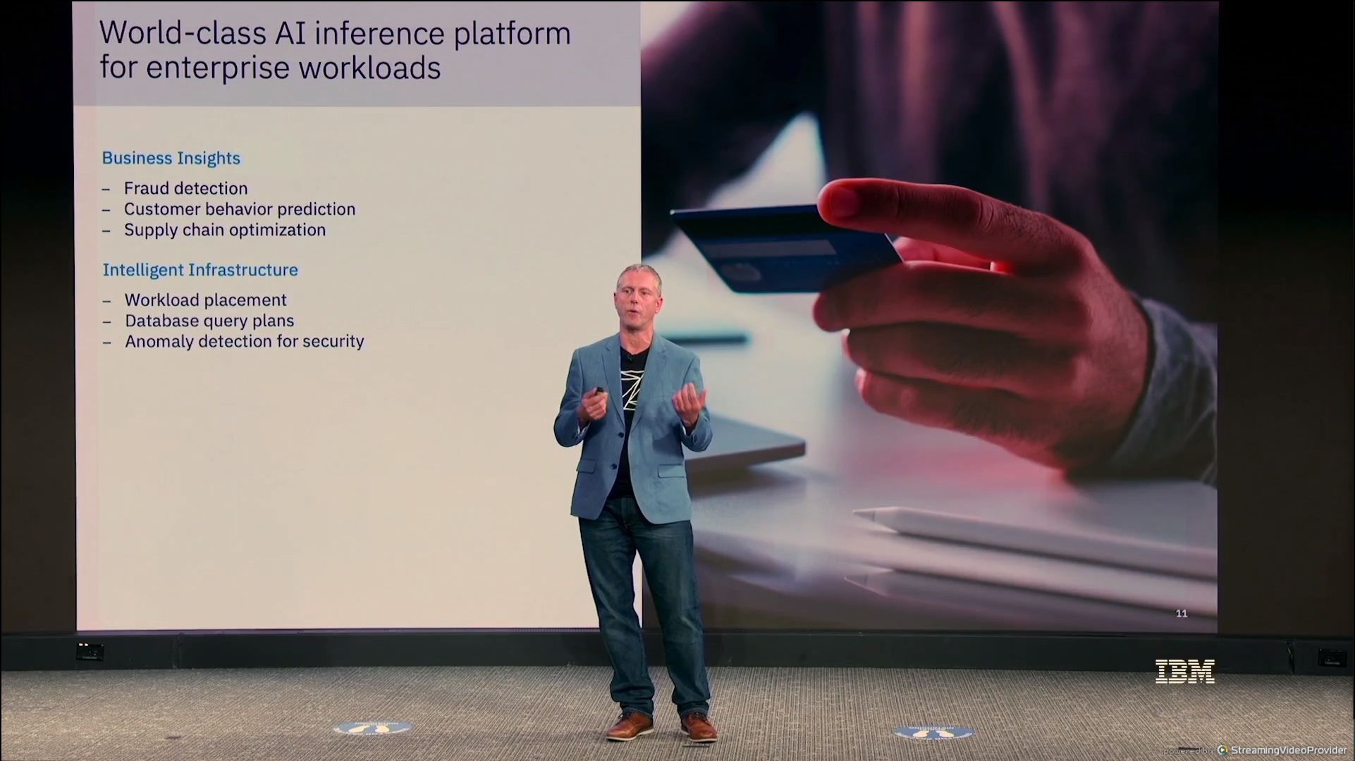
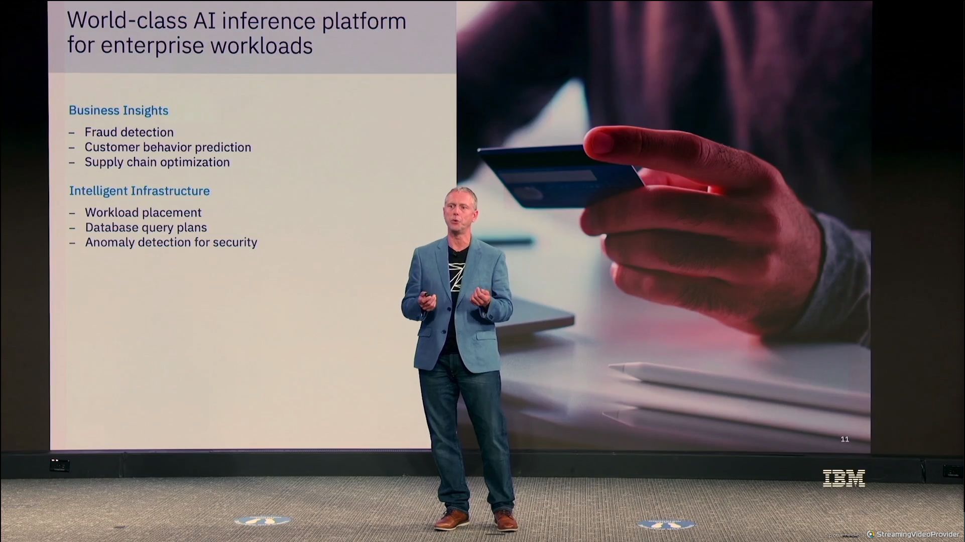
12:58PM EDT - Insights with AI models are needed
12:58PM EDT - Telum is based for this

12:59PM EDT - Enterprise workloads sensitive to ST performance and scalability
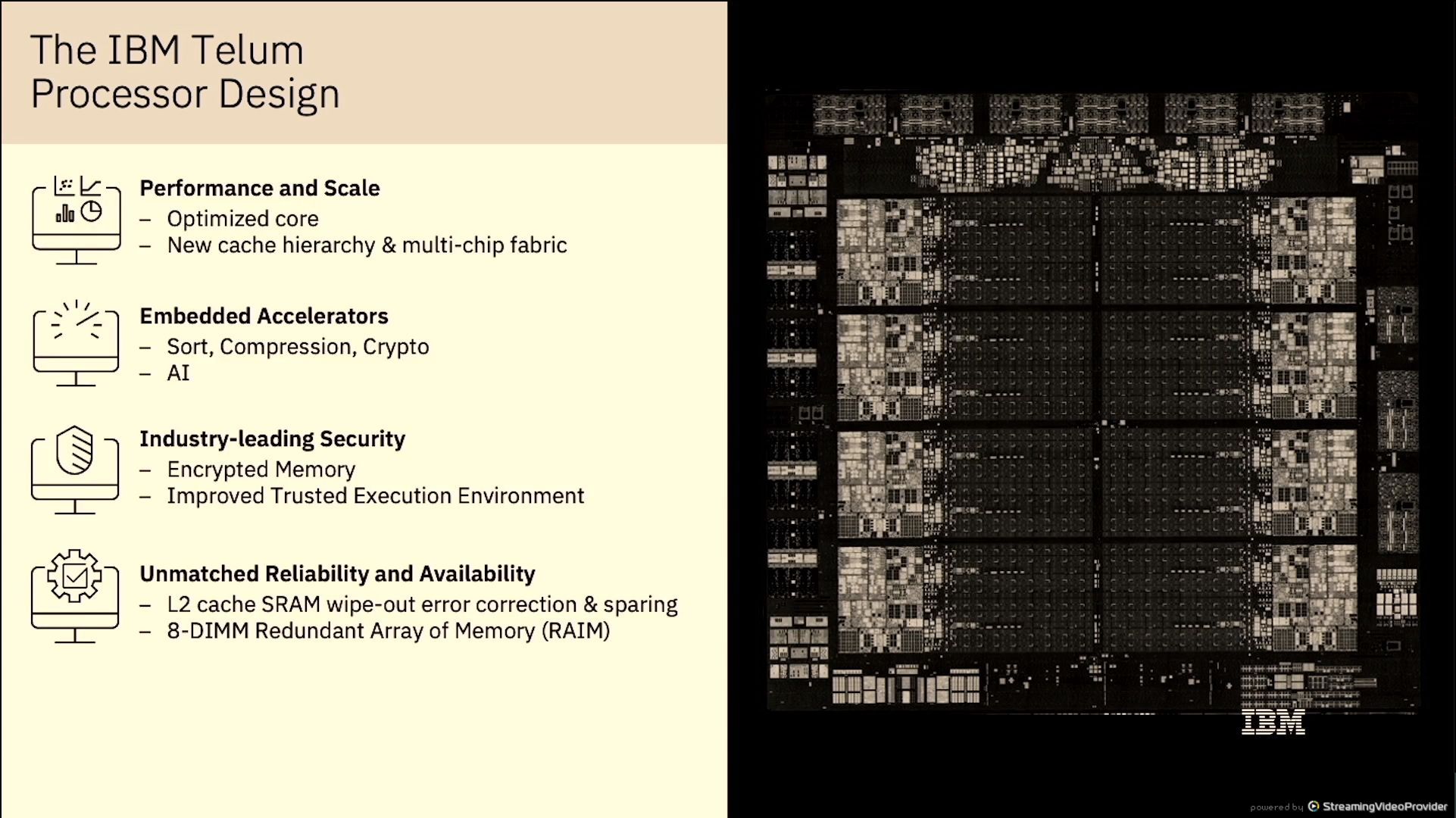
12:59PM EDT - Lots of workloads are heterogeneous
01:00PM EDT - Need embedded accelerators
01:00PM EDT - New AI accelerator
01:00PM EDT - New cache hierarchy and fabric design
01:00PM EDT - Encrypted memory and trusted execution environment
01:00PM EDT - Enclaves
01:01PM EDT - Reilability and Availability, 7x9 on z15
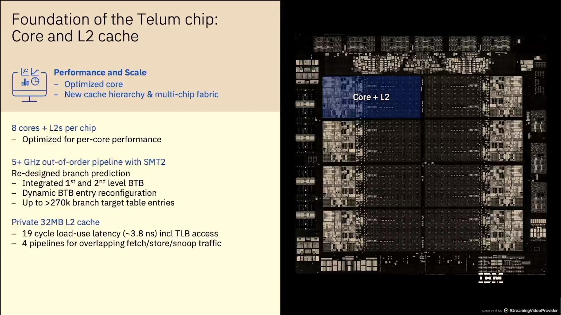
01:02PM EDT - 8 cores + 4 MB L2
01:02PM EDT - 5 GHz+ with SMT2
01:02PM EDT - New branch prediction
01:02PM EDT - 270000 branch target table entries
01:02PM EDT - Private 32 MB of L2 cache
01:03PM EDT - 19-cycle load-use latency
01:03PM EDT - Moved away for shared L3 and off-chip L4
01:04PM EDT - 4 pipelines on L2 allowing overlapped traffic
01:04PM EDT - L3 and L4 are now virtual
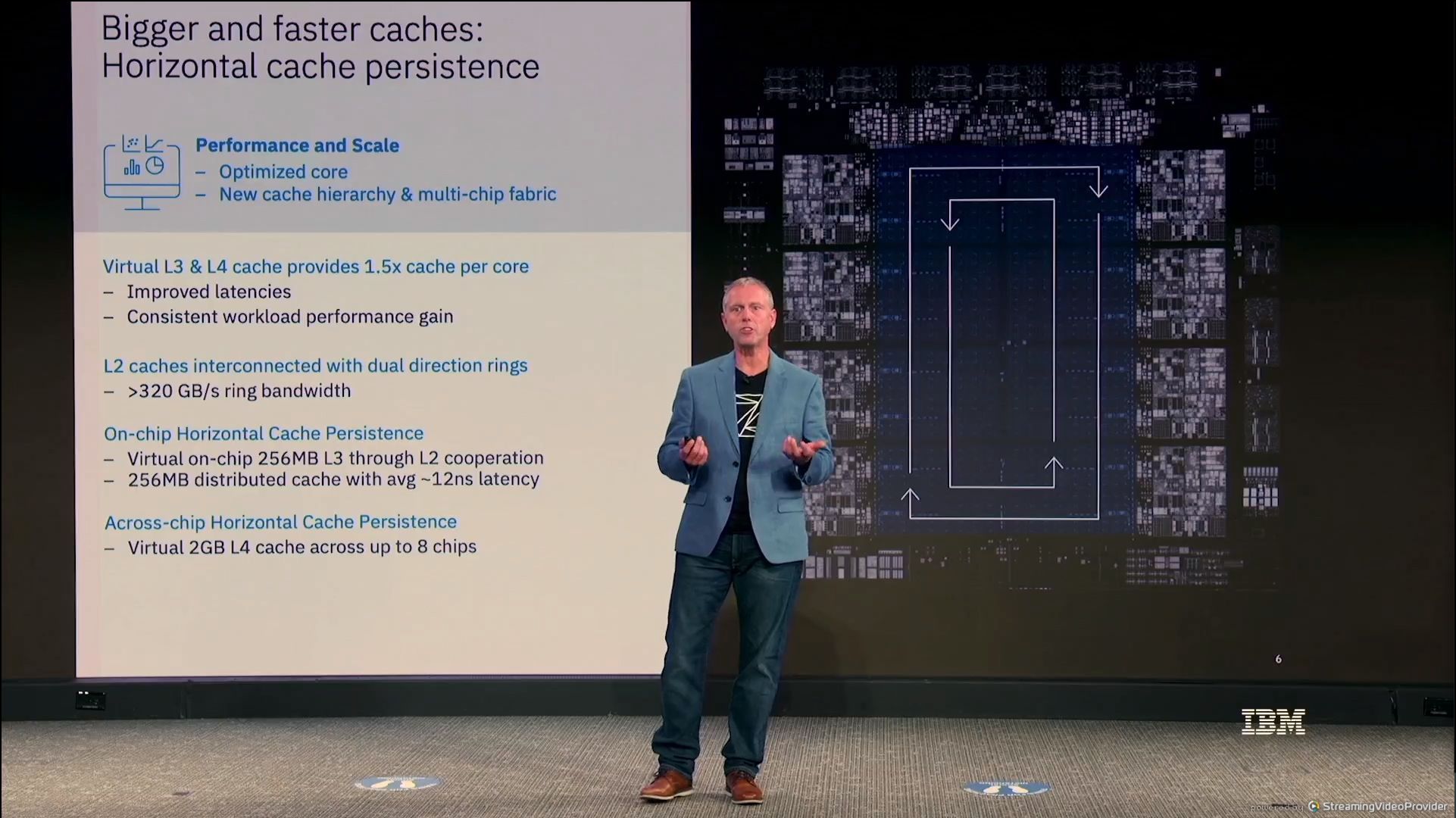
01:05PM EDT - 320 GB/s ring bandwidth
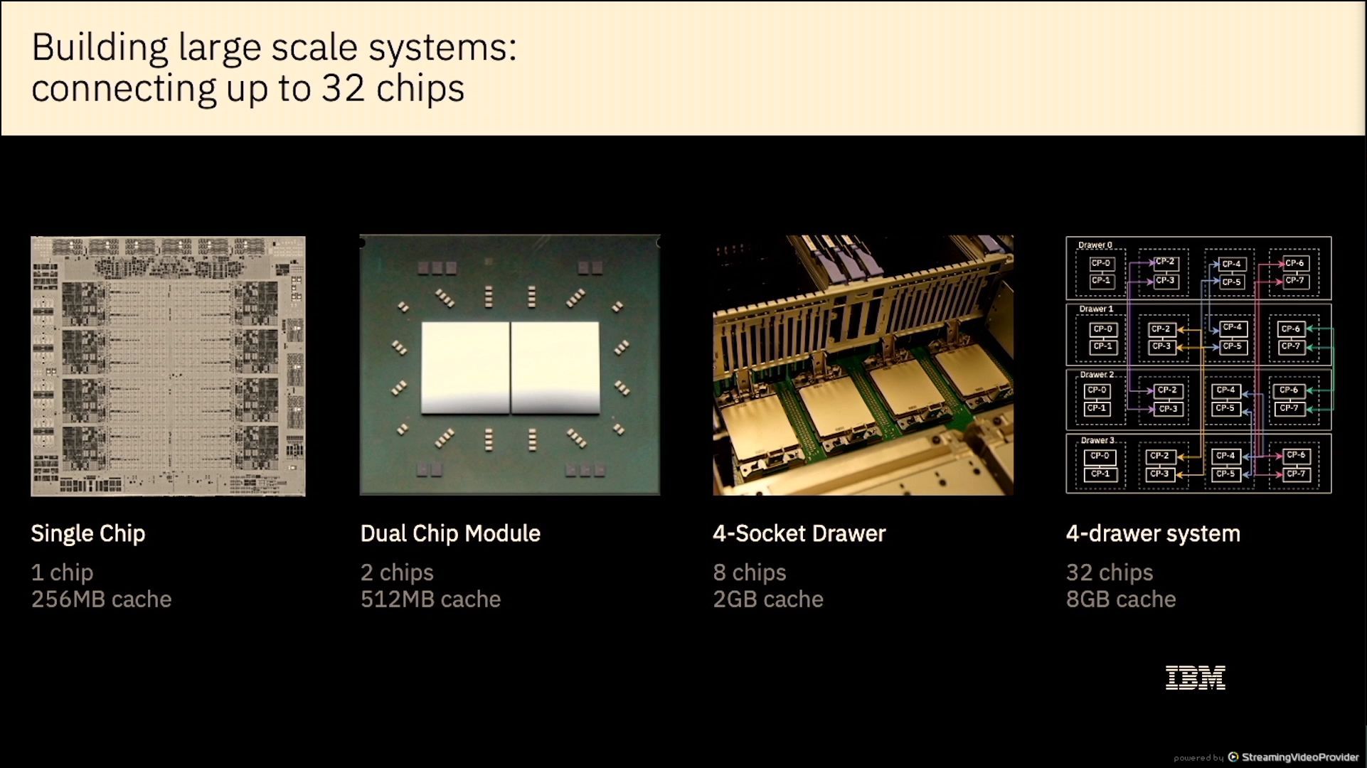
01:06PM EDT - 8 GB L4 cache

01:07PM EDT - 2-cycle transfer path between chips
01:07PM EDT - 2:1 sync clock grids
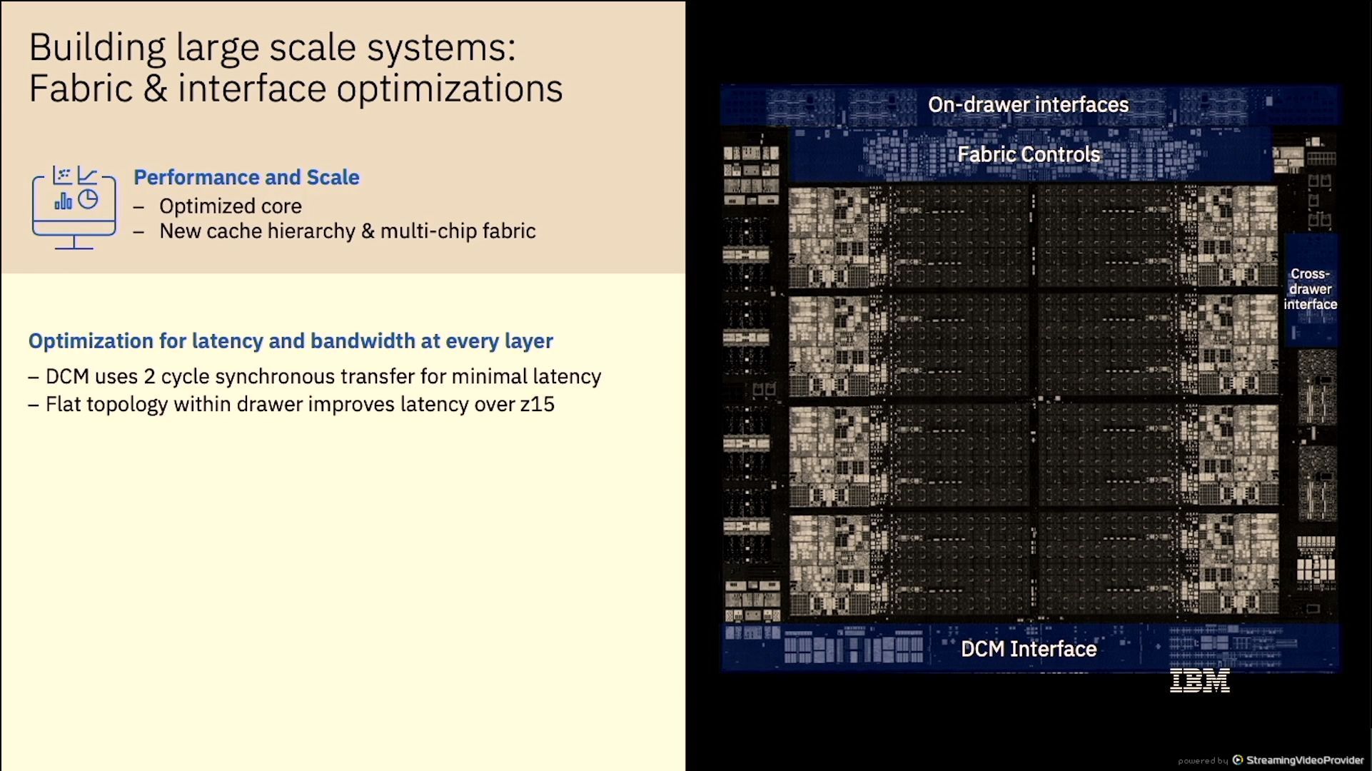
01:08PM EDT - 8-chip has flat topology - direct connect to all 8 chips
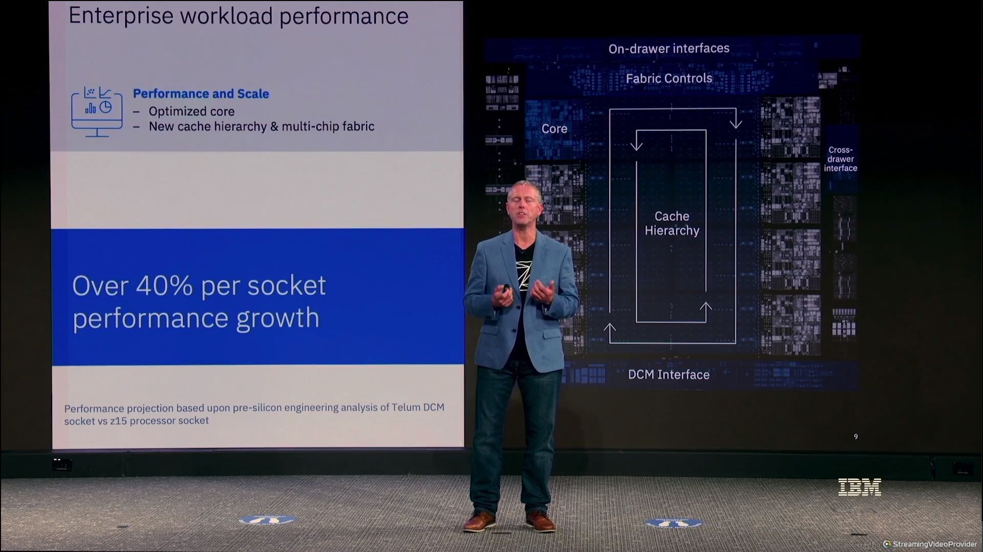
01:08PM EDT - 40% socket performance over z15
01:08PM EDT - Some of this comes from the AI workload
01:09PM EDT - AI algorithms make machines more efficient
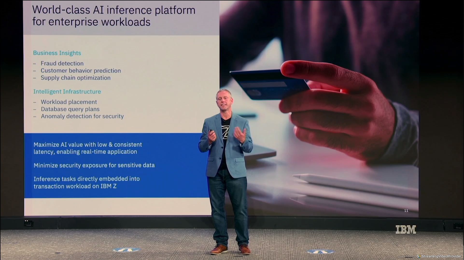
01:09PM EDT - Using the AI to increase security
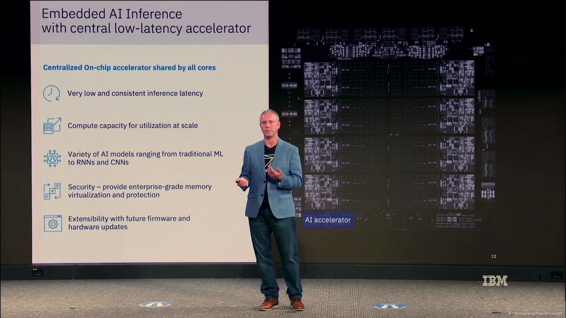
01:10PM EDT - very low inference latency - every core has access
01:11PM EDT - Kinda like the Centaur CNS core
01:12PM EDT - 6 TFLOPs per chip per AI accelerator
01:13PM EDT - Accelerator is extensible with firmware releases as AI evolves
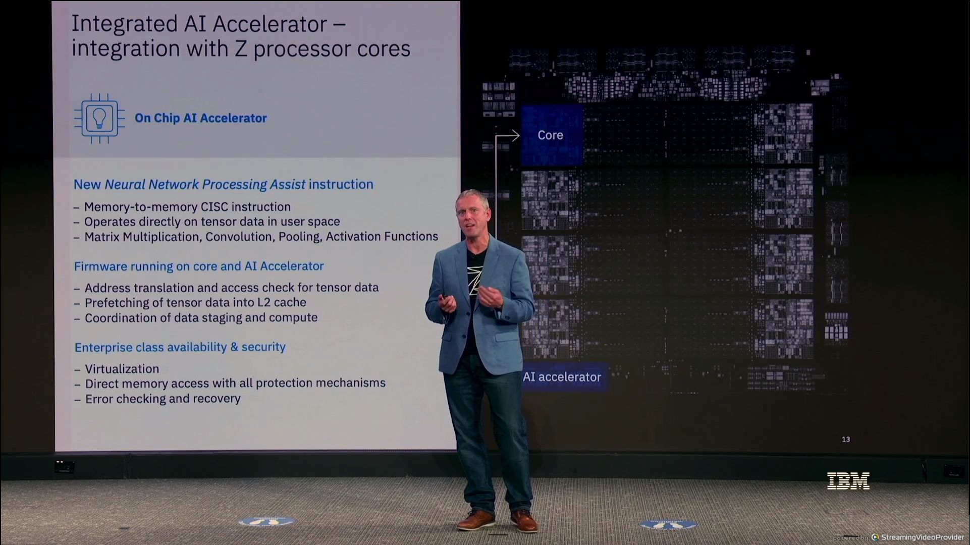
01:13PM EDT - New instructions for AI accelerator
01:13PM EDT - simpler instructions
01:13PM EDT - But you have to use the libraries to use the instructions
01:14PM EDT - supports virtualization and memory translation
01:14PM EDT - Manages all the data with the new instructions
01:14PM EDT - 6 TF per chip, 200 TF in 32-chip system
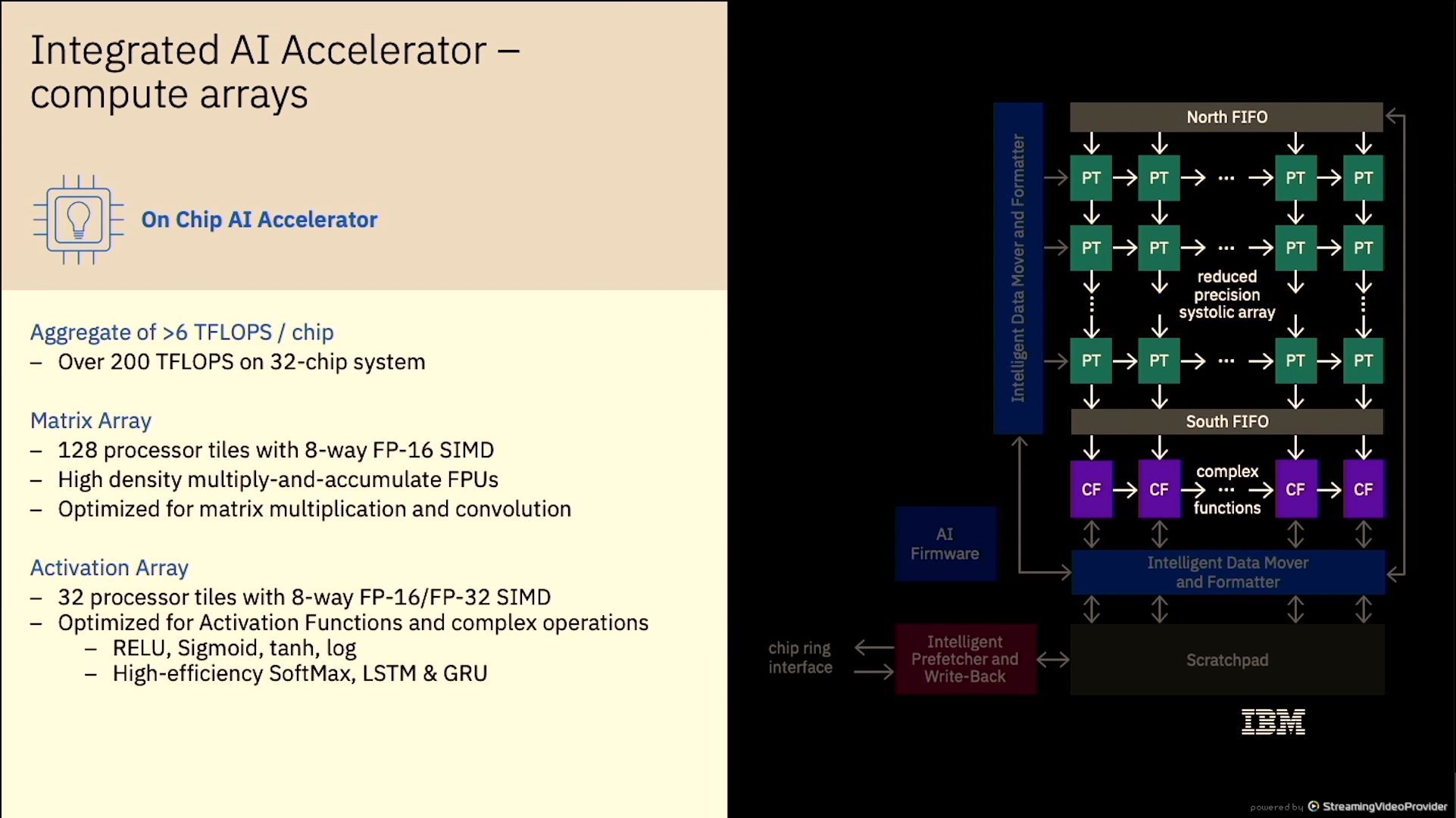
01:15PM EDT - 8-way SIMD engine, 128 tiles, MAC array on MatMul and convolution. 32 tioles for activation
01:15PM EDT - focused on FP16
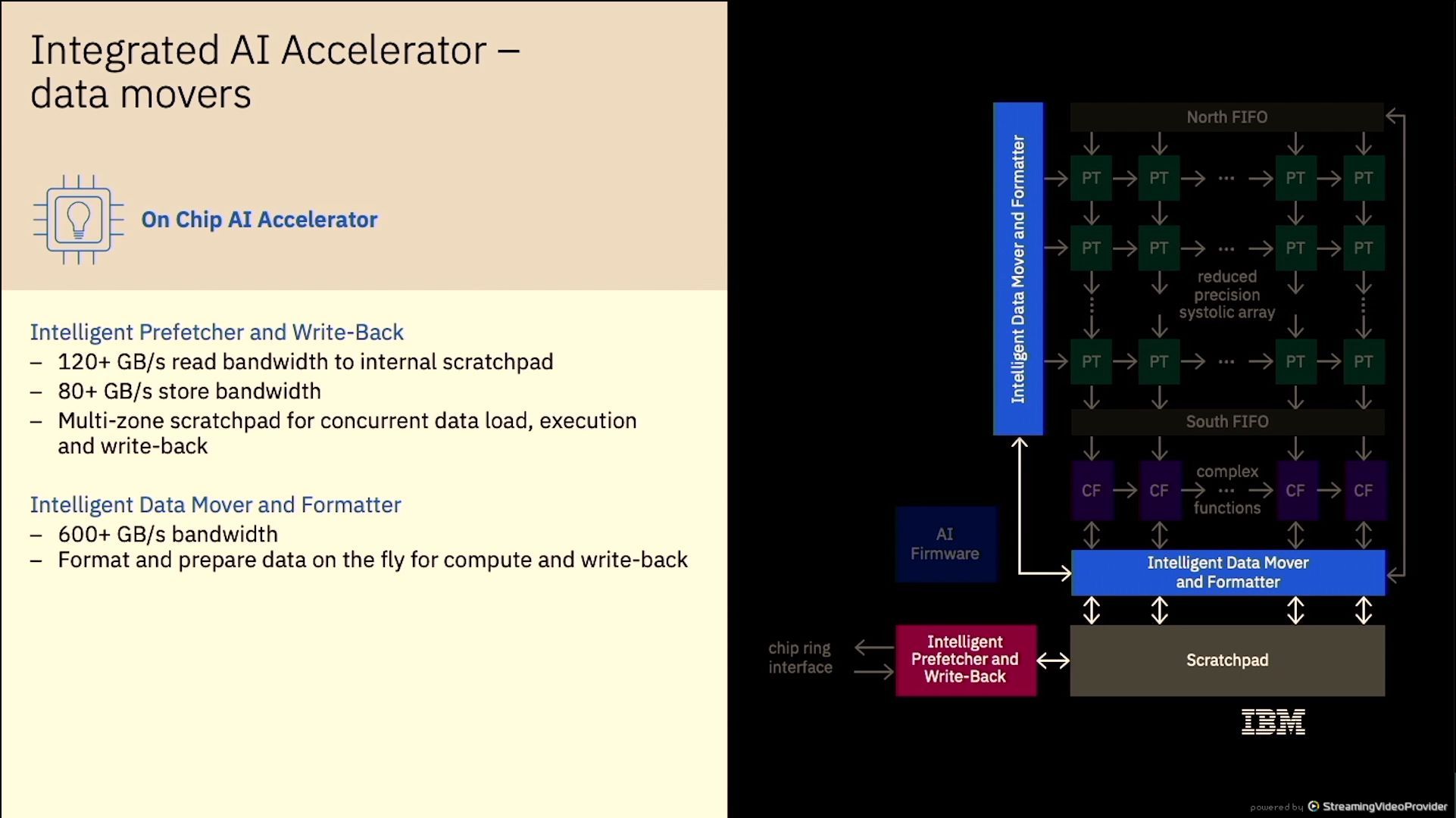
01:16PM EDT - 100 GB/s bandwidth to the AI accelerator
01:16PM EDT - 100 per core, 600 total
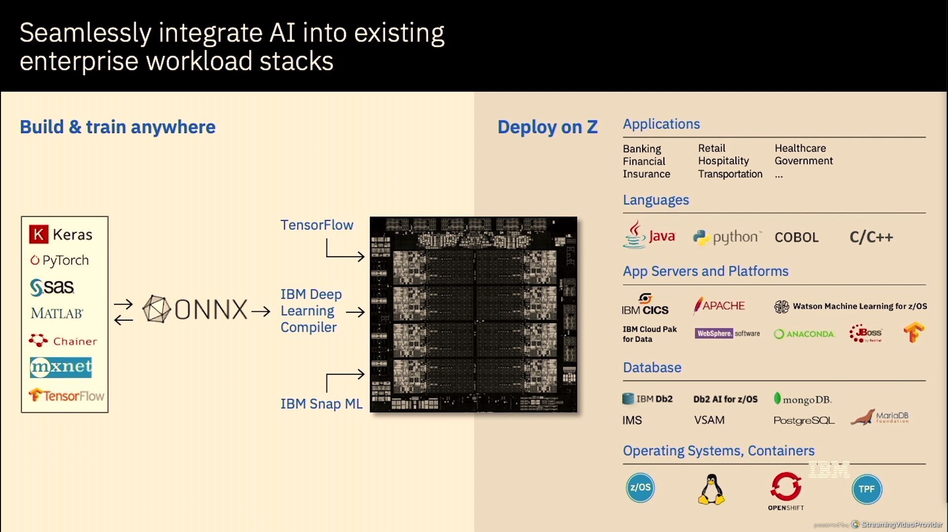
01:16PM EDT - Software is all through ONNX
01:17PM EDT - TensorFlow or through IBM Deep Learning Compiler through ONNX
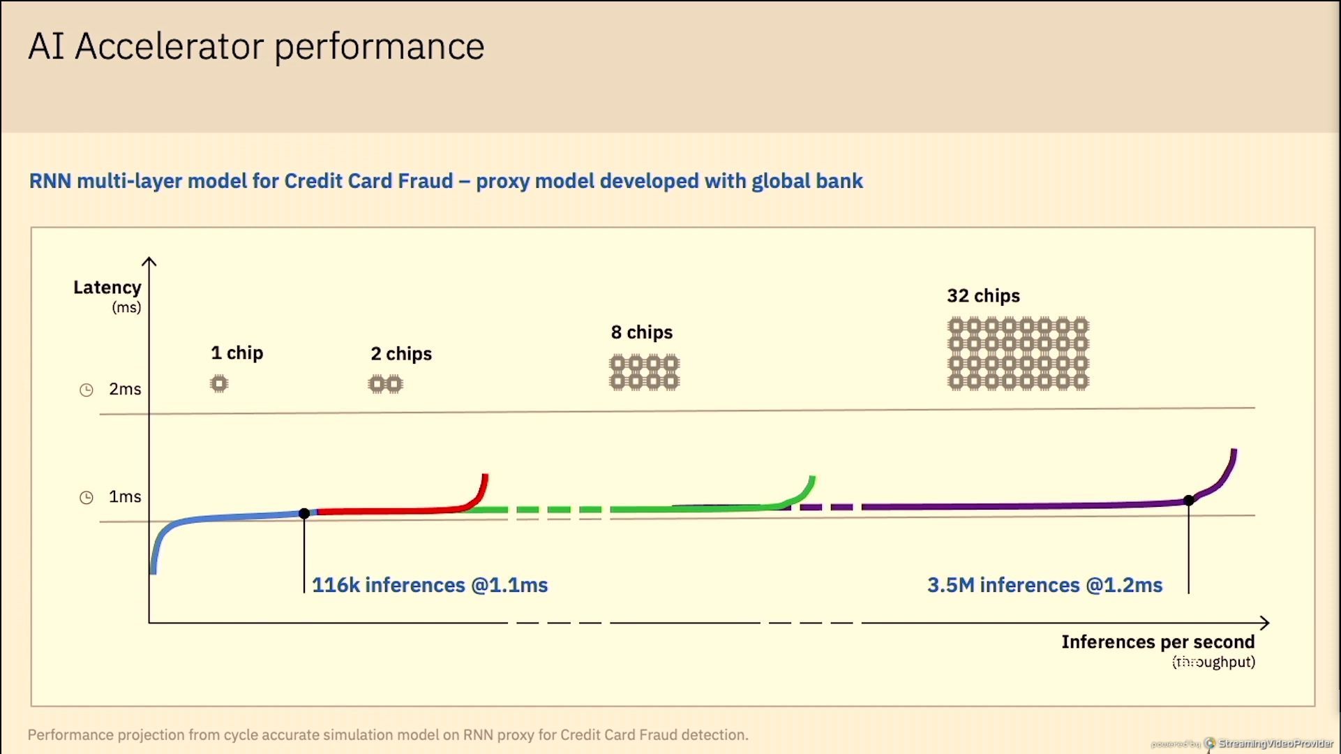
01:18PM EDT - Client proxy model performance
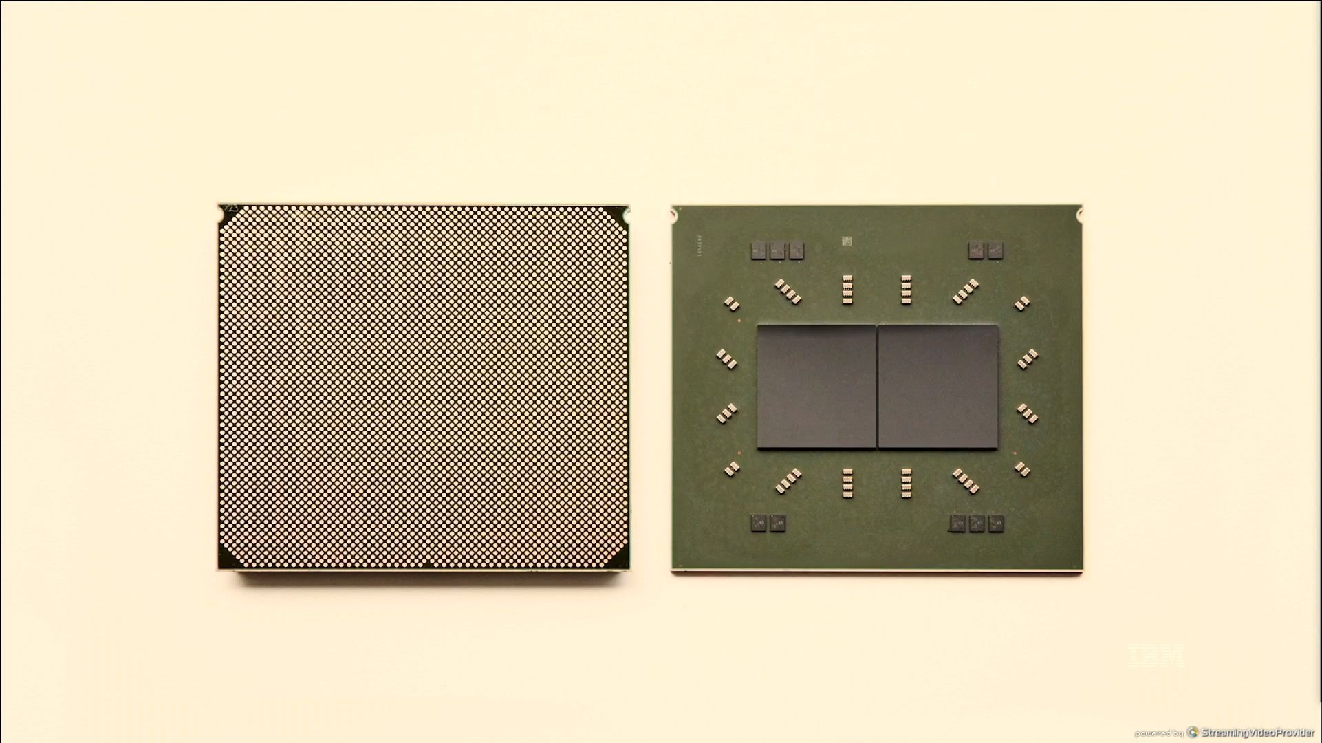
01:19PM EDT - Samsung 7nm, 530 sq mm, 22.5B transistors
01:19PM EDT - 5 GHz+ base clock frequency
01:20PM EDT - Q&A time
01:21PM EDT - Q: Use ring for AI accelerator? A: yes
01:21PM EDT - Firmware does additional management through dedicated buses
01:22PM EDT - Q: Packaing technology for dual die A: Standard, no bridges, put them close together, less than 0.5mm, some intresting thermal and mechanical, but signalling is through the package. Cool innovation on signalling due to clock synchronization.
01:23PM EDT - Q: BW of Inter-socket and Intra-drawer links A: 320 GB/s between chips, draw in each direction is 45 GB/s
01:25PM EDT - Q: Memory ordering preserved between cores and accelerators - A: magic! keep track of data, on a cache miss, broadcasts, memory state bits tracked to broadcast further out, even go across whole system, when data arrives, have to make sure it can be used, invalidate all other copies confirmed before working on data
01:29PM EDT - Q: How does Telum maintain linear scaling A: lots of scaling work on generic workloads, fabric design etc, optimize latency between chips and across drawers, that's standard. Investment in latency and bandwidth. AI chart shows almost perfect linear, because those are parallel tasks, and data is local
01:30PM EDT - Now for Sapphire Rapids from Intel


01:31PM EDT - Laucnhing 1H 22
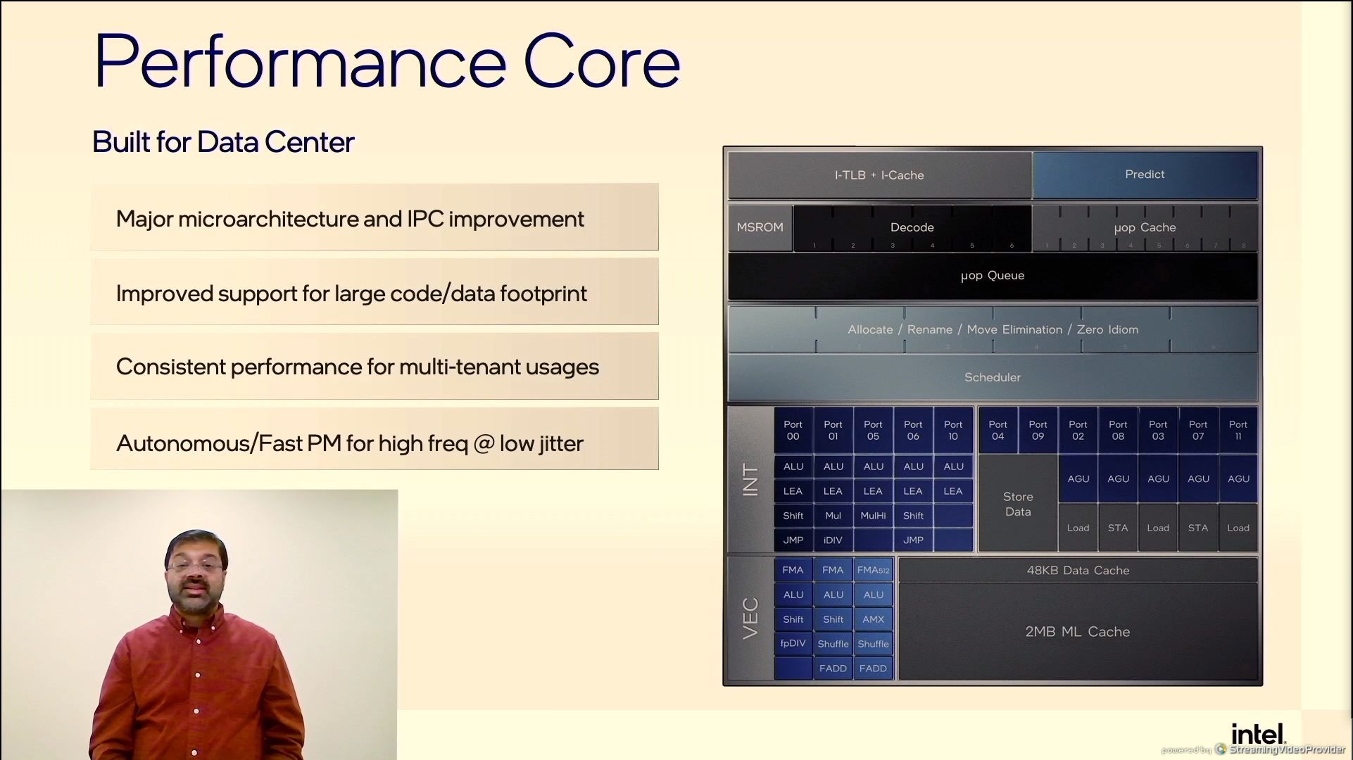
01:32PM EDT - Xeon is optimized for performance and CD Perf
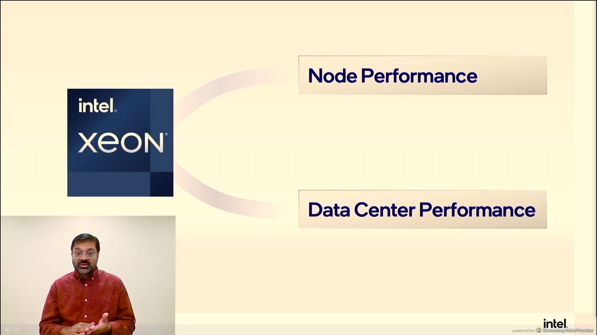
01:33PM EDT - Still calling the cores P-cores even though there's no E-cores
01:33PM EDT - Modular SoC architecture
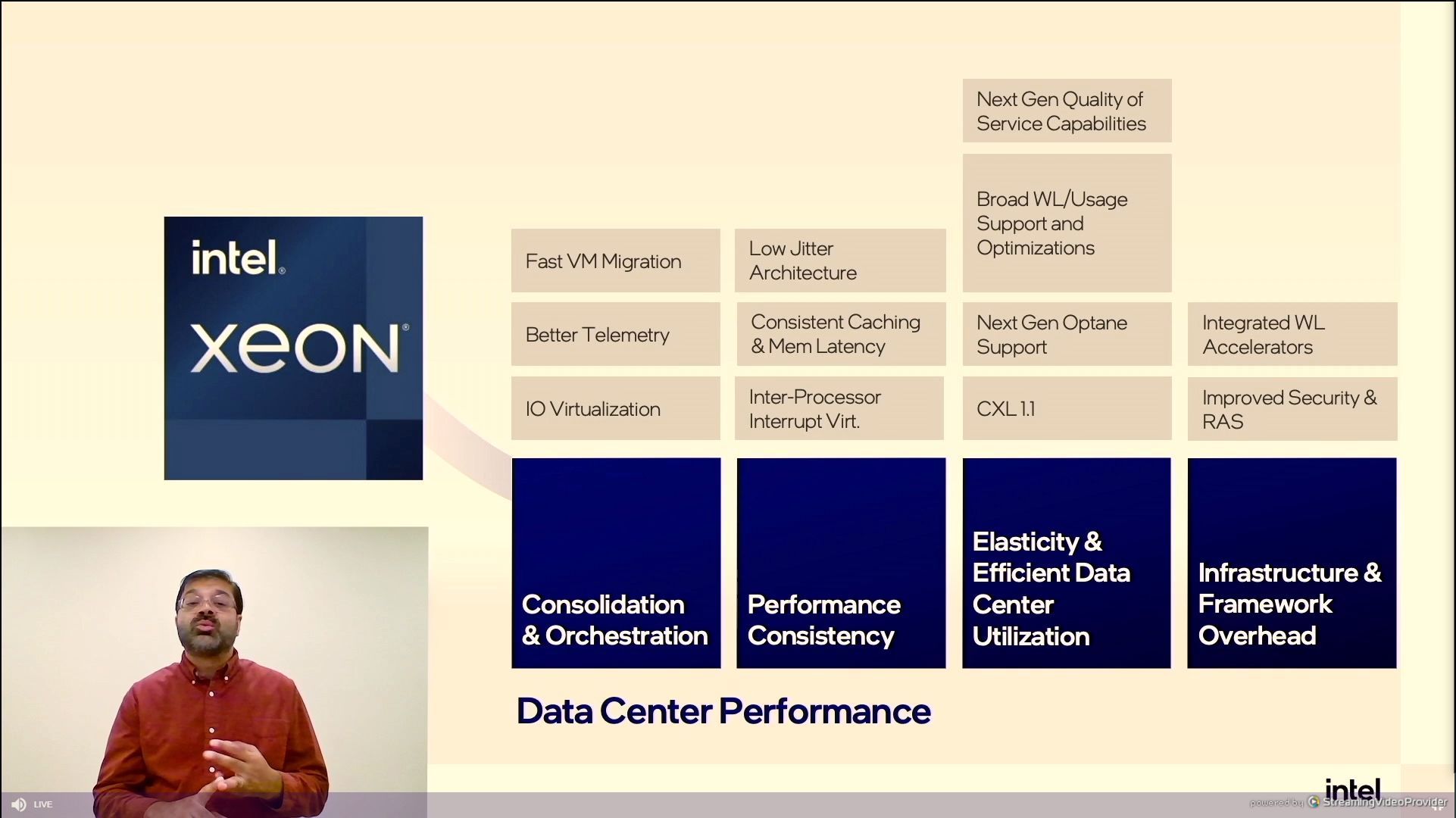
01:34PM EDT - CXL 1.1
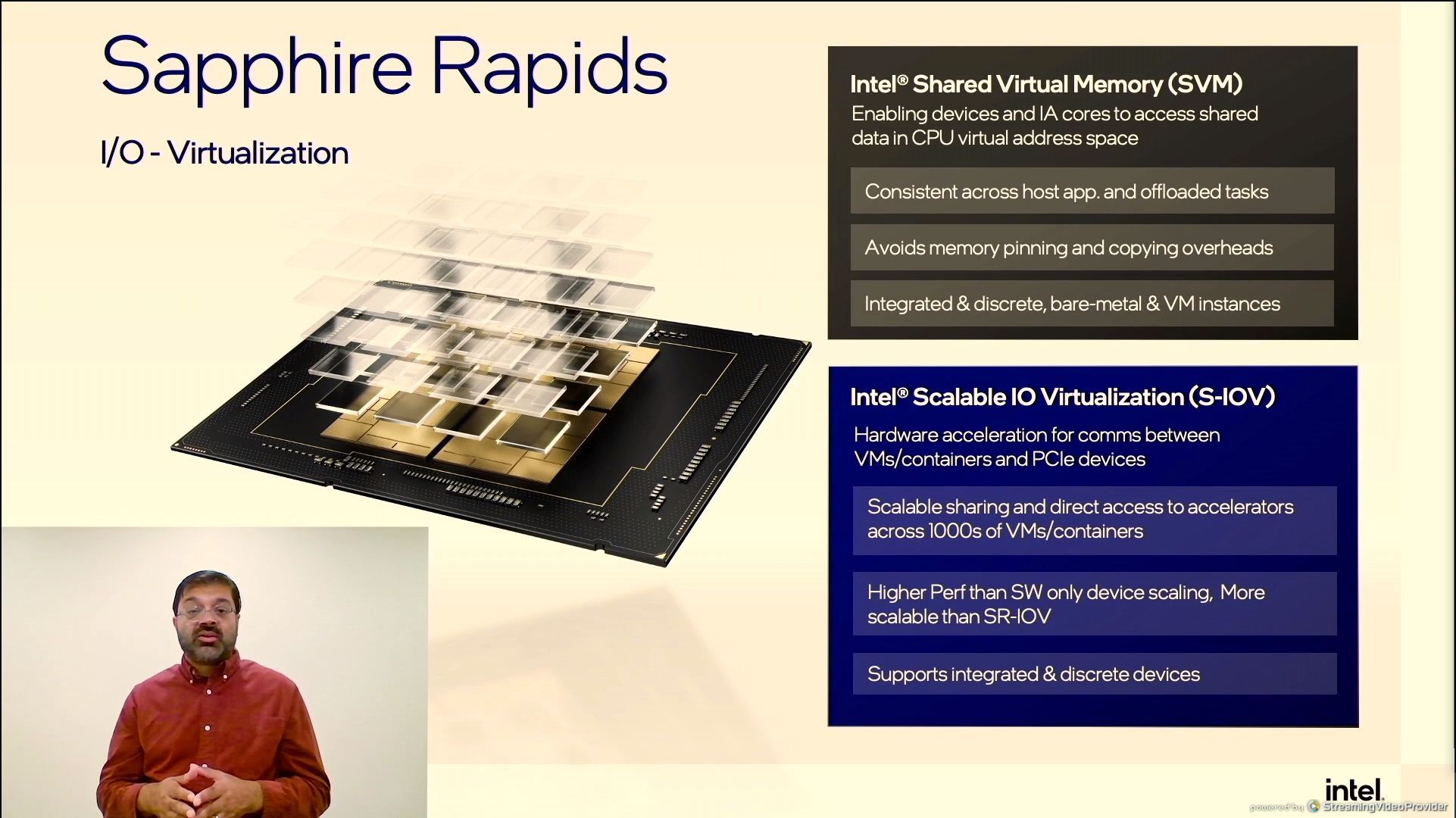
01:34PM EDT - Virtualization and VM telemetry
01:34PM EDT - Low Jitter Architecture
01:34PM EDT - Next-Gen QoS
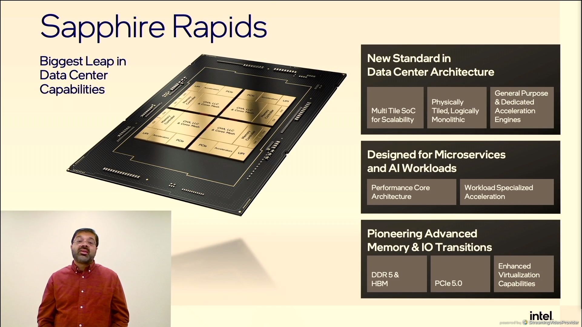
01:35PM EDT - THIS IS SAPPHIRE RAPIDS
01:35PM EDT - Here's the die shot

01:36PM EDT - We've been told there is two types of tile on SPR
01:36PM EDT - Every thread has full access to all resources on all tiles
01:37PM EDT - NUME Clustering
01:37PM EDT - NUMA*
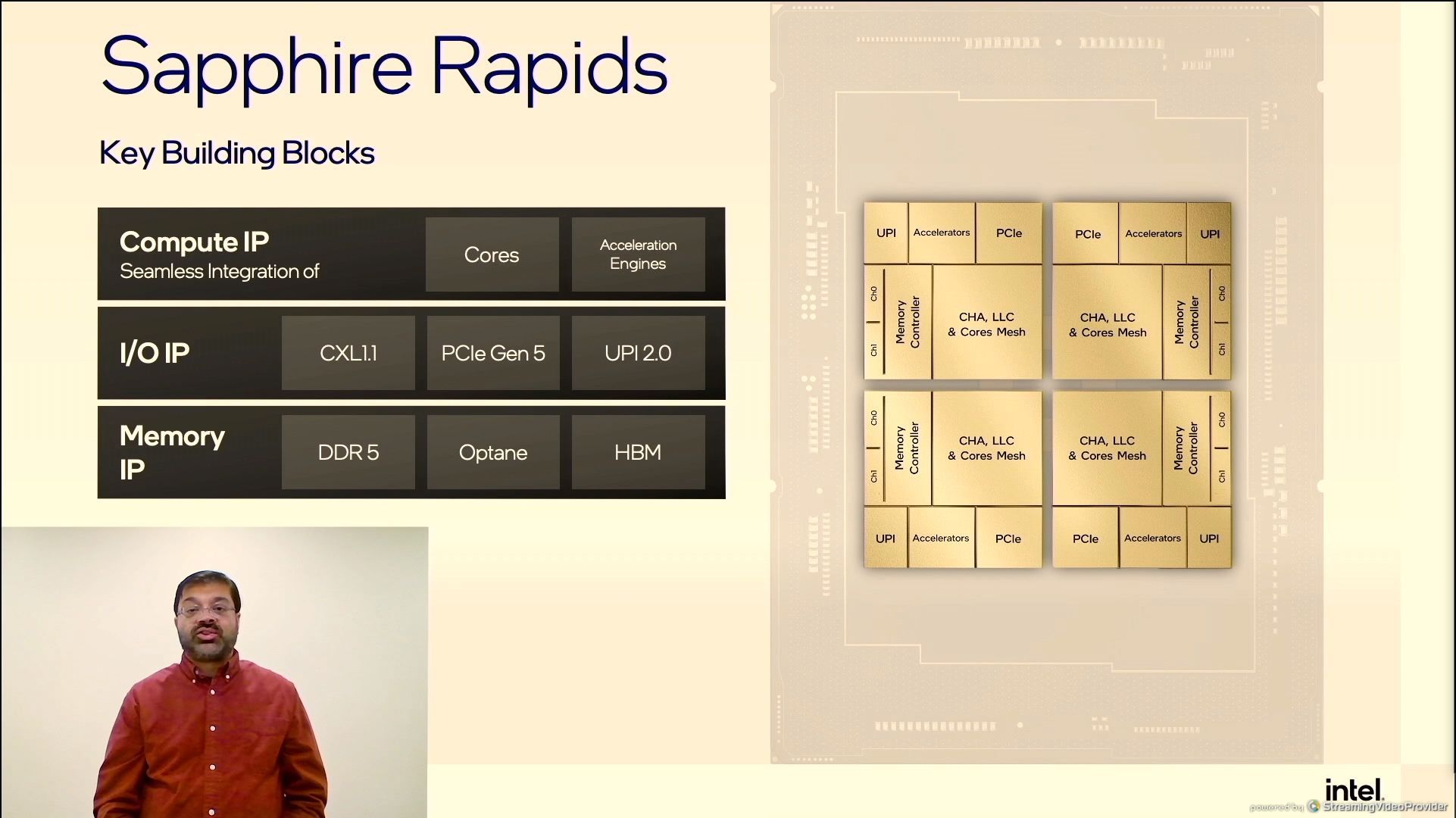
01:37PM EDT - UPI 2.0
01:38PM EDT - One of the issues here is that each tile has two memory channels - we've been told each SPR core will have 8 channels, that means each SPR product will have to have 4 tiles
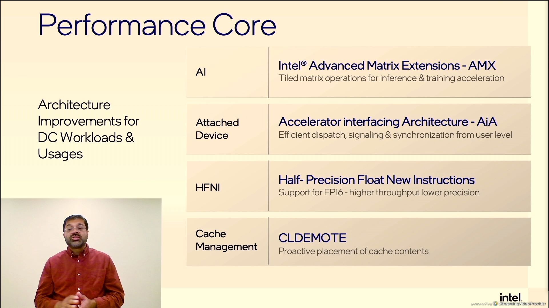
01:39PM EDT - New instructions
01:39PM EDT - AMX for Matrix
01:39PM EDT - AIA instructions for Acceelrators
01:39PM EDT - HFNI for FP16 half precision
01:39PM EDT - CLDEMOTE
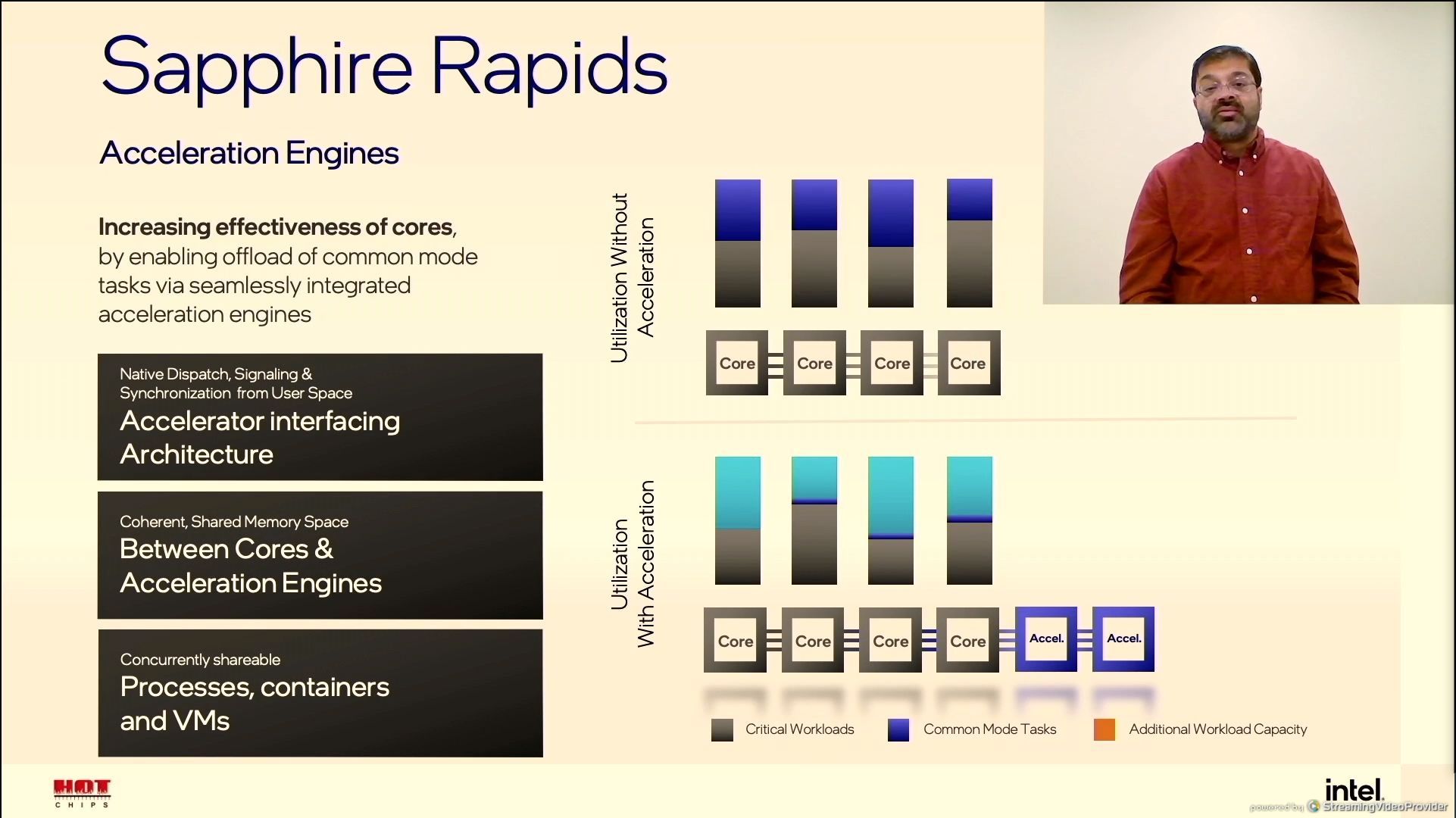
01:40PM EDT - Accelerator Engine improvements
01:41PM EDT - Avoid kernel mode overheads with AIA
01:41PM EDT - Providing base functions for deployment of acceleration engines

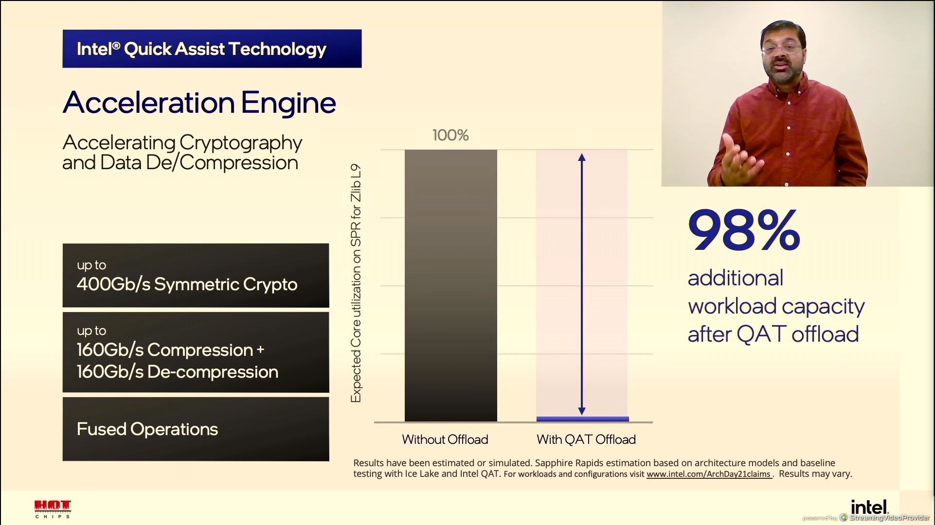
01:42PM EDT - DSA and QAT
01:42PM EDT - Doubled QAT
01:42PM EDT - Still requires a chipset
01:43PM EDT - ZLIB L9 98% offload
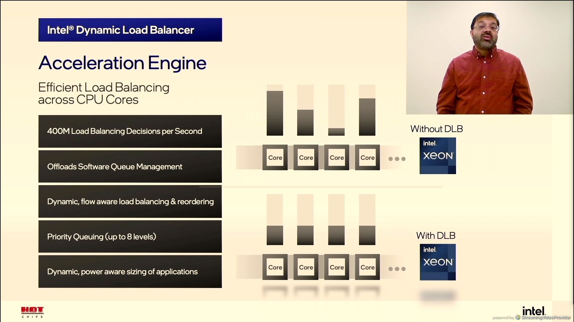
01:44PM EDT - Dynamic Load Balancer
01:44PM EDT - 400M load balancing decisions per second
01:44PM EDT - important for QoS
01:44PM EDT - ideal for packet processing and microservices
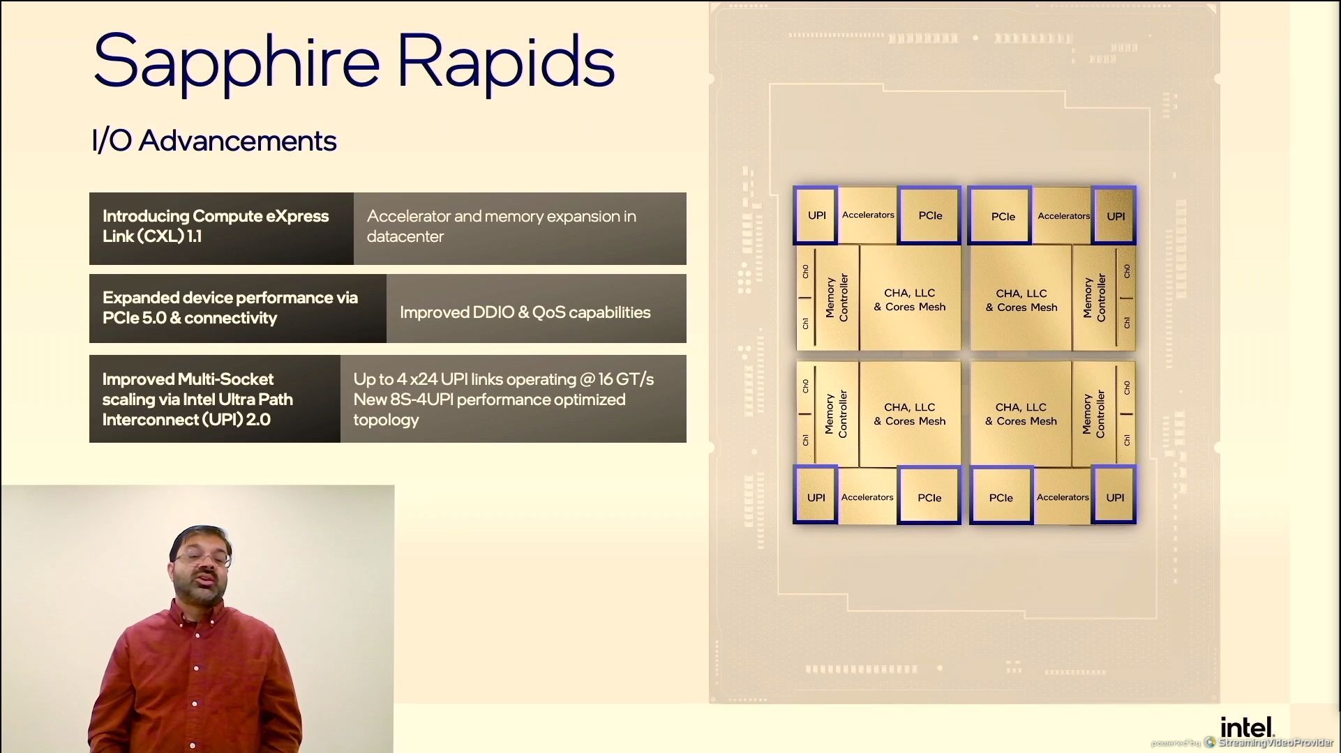
01:45PM EDT - 4 x24 UPI links at 16 GT/s (four PCIe 4.0 x16 links for multisocket)
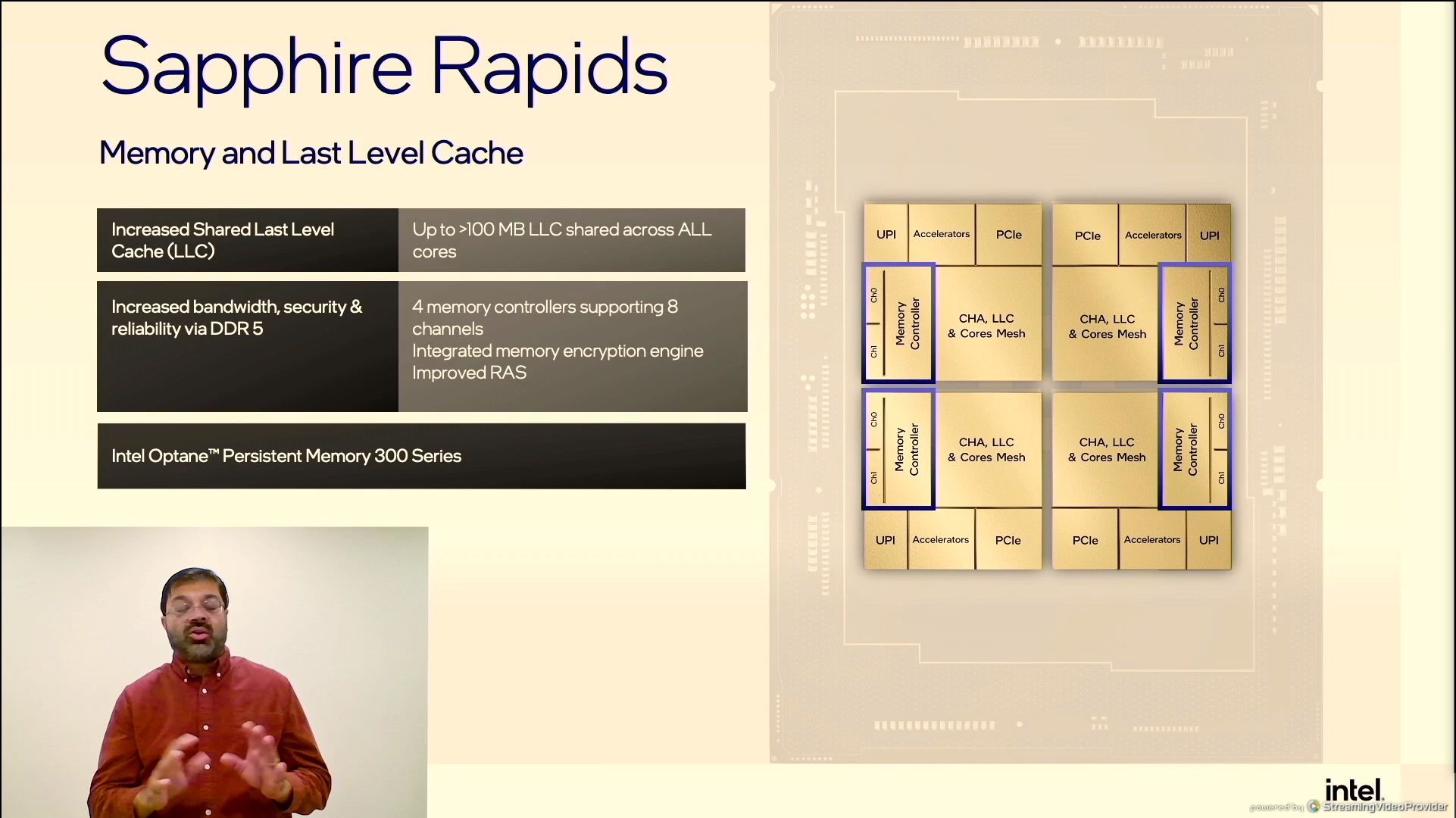
01:46PM EDT - >100 MB LLC
01:46PM EDT - 8 memory channels
01:47PM EDT - Optane 300-series support
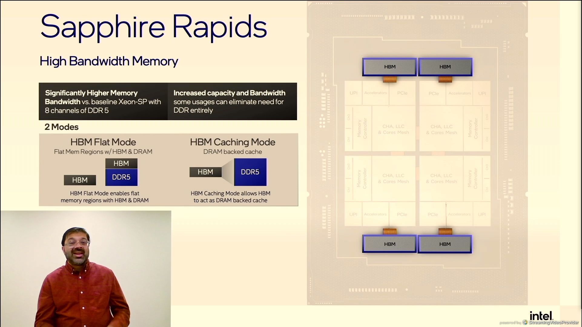
01:47PM EDT - SPR+HBM
01:47PM EDT - connected over EMIB
01:47PM EDT - Flat mode and caching mode with DRAM
01:47PM EDT - Can also support optane
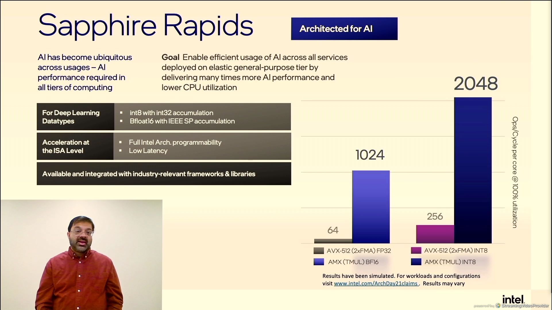
01:48PM EDT - INT8 improved through a new accelerator
01:49PM EDT - Industry standard frameworks for CPU based training and inference

01:49PM EDT - Large focus on microservices from initial design
01:50PM EDT - AIA to help service startup time
01:51PM EDT - Scalability with a monolithic view
01:51PM EDT - 10 lots of EMIB

01:51PM EDT - Q&A time
01:52PM EDT - Q: HBM Cache mode have a map? Where do you keep the tags if the HBM is a cache? A: No details quite yet
01:53PM EDT - Q: How is the AI perf of AMX compared to A100? A: No comparison yet
01:54PM EDT - Q: Intel CPU support DDIO, if HBM is cache, where does Data go first? A: Go to L3.
01:55PM EDT - Q: CXL - IBM did CAPI. Can you compare CXL to CAPI? A: Intent of CXL is similar to CAPI. CXL has IO similar to PCIe, but also can consider Accelerators with their own caches
01:55PM EDT - Intel will support CXL.mem in future products, not SPR
01:56PM EDT - Q: Interdie crossing latency A: low single digit nanosecond, little different between vertical and horizontal due to rectangular design
01:57PM EDT - DSA and QAT look like PCIe devices, require drivers (not bare metal), but they are part of the AIA framework. Works with AIA instructions, work with virtualization, but they look like PCIe devices
02:00PM EDT - .


39 Comments
View All Comments
schujj07 - Monday, August 23, 2021 - link
Anyone else look at Sapphire Rapids and think the layout is eerily similar to Epyc Gen 1. Almost looks like Intel wasn't ready to go full chiplet like Zen2 or later and could only do MCM.WaltC - Monday, August 23, 2021 - link
First thing I thought of...;)Oxford Guy - Monday, August 23, 2021 - link
I was very excited about Sapphire Rapids until I saw that it’s ‘glued together’.Yojimbo - Monday, August 23, 2021 - link
I think Intel's marketing objections to gen 1 Epyc was that they were "glued together" desktop parts, not that they were using MCMs. Intel has been planning for MCMs for a long time. And the way Intel is gluing together their MCMs in Sapphire Rapids is more sophisticated than how AMD did for gen 1 Epyc.arashi - Monday, August 23, 2021 - link
After just about half a decade later I sure hope so.Yojimbo - Monday, August 23, 2021 - link
Epyc is connected through the PCB, Sapphire Rapids uses EMIB. Intel has been developing EMIB for probably a decade, and they've been talking about using packaging technologies to maintain a Moore's Law-like pace of improvement in application performance for years.Chiplet is just what AMD calls their CPU MCM.
sgeocla - Tuesday, August 24, 2021 - link
EMIB and Foveros are at least 2 years behind what TSMC & AMD are doing. See Intel current 50 micron bump pitch and 10 micron pitch in 2023-2024 for TSV connections vs 9 micron pitch used for 3D V-cache for AMD with Cu-Cu bonding using lower power.They difference between AMD's approach and Intel's approach is that one of them is efficient and cost effective and has been shipping in millions of devices while the other has only been demonstrated in expensive, low volume and low performance products like Lakefield.
AMD's are using chiplets on multiple nodes with the best characteristics of each. Intel is using MCM for sapphire rapids because they only have 1 base tile on 10nm, mirrored and rotated. This means low yields and that the tiles can't be salvaged for different products like AMD does with Ryzen and Threadripper. This is basically EPYC1 only with smarter glue. That's why it's limited to 56 cores while AMD's Genoa will be 96 cores with Genoa X at 128 cores.
AMD resolved the issue of effectiev latency using larger caches but Intel can't go higher in cores because their architecture means their latency increases with the number of cores.
schujj07 - Tuesday, August 24, 2021 - link
While EMIB might be the connection, I wouldn't be surprised if Intel runs into the same problems with Sapphire Rapids that AMD had with Epyc 1, ie latency across to different chips. Each tile has 2 its own 2 channel memory controller. Therefore local memory requests will be quick, however, when you need to go to something in a different tile the data will have to traverse the mesh/UPI links. AMD got around this in Gen 2 & 3 by having the IO die. That centralized all IO & memory communication. I I just think that Intel is 4-5 years behind AMD in terms of layout on their chips. Granted we won't know until it ships supposedly in H1 2022.whatthe123 - Tuesday, August 24, 2021 - link
Epyc 1 was worse performing because it was on a worse node and had slow single hop i/o paths between CCXs instead of an IOD. Cache access was also limited to each 4 core ccx. Intel is claiming EMIB wiring is similar to monolithic performance and that all cores have access to all resources, which would be very different from Naples. Claiming something isn't the same as actually delivering so who knows if the real world performance is any good but based on what they're saying it wouldn't have the same downsides as Naples.abufrejoval - Wednesday, August 25, 2021 - link
"the PCB" is too easy to misconstrue as the mainboard. The die carrier used here is a rather special PCB, which doesn't duplicate a typical PCB's latencies, capacities and voltage levels.