Startup Showcases 7 bits-per-cell Flash Storage with 10 Year Retention
by Dr. Ian Cutress on December 15, 2021 11:30 AM EST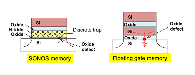
One of the key drivers to increase capacity in next generation storage has been to increase the number of bits that can be stored per cell. The easy jump of one to two bits-per-cell gives a straight 100% increase, in exchange for more control needed to read/write the bit but also limits the cell endurance. We’ve seen commercialization of storage up to four bits-per-cell, and talk about five. A Japanese company is now ready to start talking about their new 7 bits-per-cell solution.
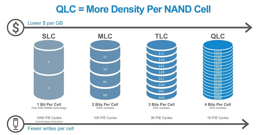
Image courtesy of Plextor, up to 4 bits-per-cell
Moving from one to two bits-per-cell gives an easy doubling of capacity, and moving to three bits-per-cell is only another 50% increase. As more bits are added, the value of adding those bits diminishes, but the cost in the equipment to control the read and writes increases exponentially. There has to be a medium balance between how many bits-per-cell makes economic sense, and how much the control electronics costs to implement to enable those bits.
- 1 bit per cell requires detection of 2 voltage levels, base capacity
- 2 bit per cell requires detection of 4 voltage levels, +100% capacity
- 3 bit per cell requires detection of 8 voltage levels, + 50% capacity
- 4 bit per cell requires detection of 16 voltage levels, +33% capacity
- 5 bit per cell requires detection of 32 voltage levels, +25% capacity
- 6 bit per cell requires detection of 64 voltage levels, +20% capacity
- 7 bit per cell requires detection of 128 voltage levels, +16.7% capacity
Also, the more bits-per-cell, the lower the endurance – the voltage variation when you store many bits only has to drift slightly to get the wrong result, and so repeated read/writes to a high capacity cell will make that voltage drift until the cell is unusable. Right now the market seems happy with three bits-per-cell (3bpc) for performance and four bits-per-cell (4bpc) for capacity, with a few 2bpc designs for longer term endurance. Some of the major vendors have been working on 5bpc storage, although the low endurance may make the technology only good for WORM – write once, read many, which is a common acronym for the equivalent of something like an old-school CD or non-rewritable DVD.

Floadia Corp., a Series C startup from Japan, issued a press release this week to state that it has developed storage technology capable of seven bits-per-cell (7bpc). Still in the prototype stage, this 7bpc flash chip, likely in a WORM scenario, has an effective 10-year retention time for the data at 150C. The company says that a standard modern memory cell with this level of control would only be able to retail the data for around 100 seconds, and so the secret in the design is to do with a new type of flash cell they have developed.
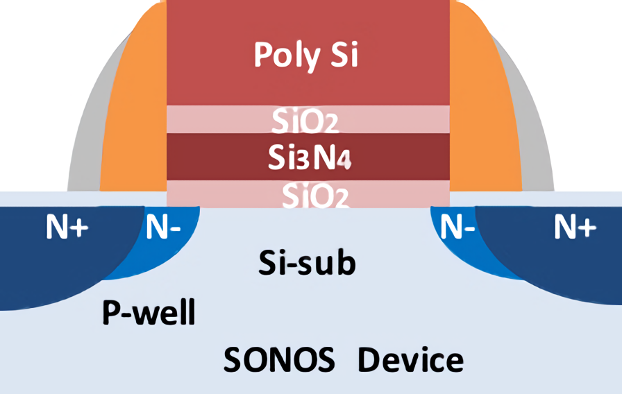
The SONOS cell uses a distributed charge trap design relying on a Silicon-Oxide-Nitride-Oxide-Silicon layout, and the company points to an effective silicon nitride film in the middle where the charges are trapped to allow for high retention. In simple voltage program and erase cycles, the company showcases 100k+ cycles with a very low voltage drift. The oxide-nitride-oxide layers rely on SiO2 and Si3N4, the latter of which is claimed to be easy to manufacture. This allows a non-volatile SONOS cell to be used in NV-SRAM or embedded designs, such as microcontrollers.
It’s actually that last point which means we’re a long time from seeing this in modern NAND flash. Floadia is currently partnering with companies like Toshiba to implement the SONOS cell in a variety of microcontrollers, rather than large NAND flash deployments, at the 40nm process node as embedded flash IP with compute-in-memory properties. Those aren’t at 7 bits-per-cell yet, to the effect that the company is promoting that two cells can store up to 8-bits of network weights for machine learning inference – when we get to 8 bits-per-cell, then it might be more applicable. The 10-year retention of the cell data is where it gets interesting, as embedded platforms will use algorithms with fixed weights over the lifetime of the product, except for the rare update perhaps. Even with increased longevity, Floadia doesn’t go into detail regarding cyclability at 7bpc at this time.
An increase from modern 3bpc to 6bpc NAND flash would afford a double density increase, however larger cells would be needed, which would negate the benefits. There’s also the performance aspect if the development of >4bpc ever made it to consumers, which hasn’t been touched upon.
It will be an interesting technology to follow.
Source: Floadia Press Release


48 Comments
View All Comments
Kamen Rider Blade - Wednesday, December 15, 2021 - link
The Write Endurance on these gotta suckWereweeb - Wednesday, December 15, 2021 - link
The question is: can it be adapted to 3D NAND processes?nandnandnand - Wednesday, December 15, 2021 - link
If it can't, there's absolutely no point in using it since you could use 3D + 1 bit per cell (SLC) instead.dwillmore - Wednesday, December 15, 2021 - link
As soon as I saw 7 BPC, I knew it wasn't going to be manufactured in any kind of advanced process. To be able to reliably store enough electrons to even be able to tell apart 128 different voltage levels, you'd physically need a large area--especially with the insulation thickness you'd need to get that 10y at 150C retention. Then they mentioned using it in microcontrollers and similar applications at 40nm and I was all "...and there it is."Might as well lump this in with FERAM and similar technologies that only make sense in very constrained applications.
BushLin - Sunday, December 19, 2021 - link
Isn't most NAND at 40nm, for endurance and it's become a race for how many layers can be stacked?mode_13h - Monday, December 20, 2021 - link
> Isn't most NAND at 40nmNoooo... not for a long time. There's been competition in both areal density *and* number of layers.
UpSpin - Friday, December 17, 2021 - link
I doubt the article is correct.Form 1-bit to 2-bit I need 100% more bits, and double the capacity at the same time, from 1 state I can store 2 states.
From 2-bit to 3-bit I only need 50% more bits, but still double the capacity, instead of 2 states I can store 4 states.
From 3-bit to 4-bit I only need 25% more bits, but again double the capacity, instead of 4 states I can store 8 states now.
....
So in case of 7-bit I can store 128 states (the reason I need to distinguish 128 voltage levels). So the point of the article is totally wrong. The more bits I add the cheaper it gets.
mode_13h - Saturday, December 18, 2021 - link
> From 2-bit to 3-bit I only need 50% more bits, but still double the capacity,> instead of 2 states I can store 4 states.
Doubling the number of states doesn't equate to doubling the storage capacity. I don't know what else to say, other than maybe try reading about information theory and some of it'll start to sink in?
> So the point of the article is totally wrong. The more bits I add the cheaper it gets.
I think that point isn't lost on anyone. The issue is that the incremental benefit of each further bit grows less and less. At some point, it's not worth the tradeoffs that come with packing more bits per cell.
mode_13h - Saturday, December 18, 2021 - link
As I was reading this, I got to wondering... does anyone know if conventional NAND does anything like storing a "full" cell per block, as a reference charge? When reading the block, you could use that to calibrate the ADC, essentially normalizing out the voltage drop due to charge leakage.bob27 - Saturday, December 18, 2021 - link
I'm not a physicist or electrical engineering person, but I assume voltage drift would occur statistically randomly. I.e. something that lets you determine in advance the average drift of a bunch of cells, but not the particular drift of a particular cell.