TSMC: N2 To Start With Just GAAFETs, Add Backside Power Delivery Later
by Anton Shilov on June 29, 2022 12:00 PM EST- Posted in
- Semiconductors
- TSMC
- GAAFET
- 2nm
- N2
When TSMC initially introduced its N2 (2 nm class) process technology earlier this month, the company outlined how the new node would be built on the back of two new cutting-edge fab techniques: gate-all-around transistors, and backside power rails. But, as we've since learned from last week's EU symposium, TSMC's plans are a bit more nuanced than first announced. Unlike some of their rivals, TSMC will not be implementing both technologies in the initial version of their N2 node. Instead, the first iteration of N2 will only be implementing gate-all-around transistors, with backside power delivery to come with a later version of the node.
So far, TSMC has mentioned two distinctive features of N2: nano sheet gate-all-around (GAA) transistors, and backside power rails. GAA transistors have two unique advantages over FinFETs: they solve many challenges associated with the leakage current since GAAFET's channels are horizontal and are surrounded by gates around all four sides. Meanwhile, backside power rail enabled improved power delivery to transistors, which increases performance and lowers power consumption.
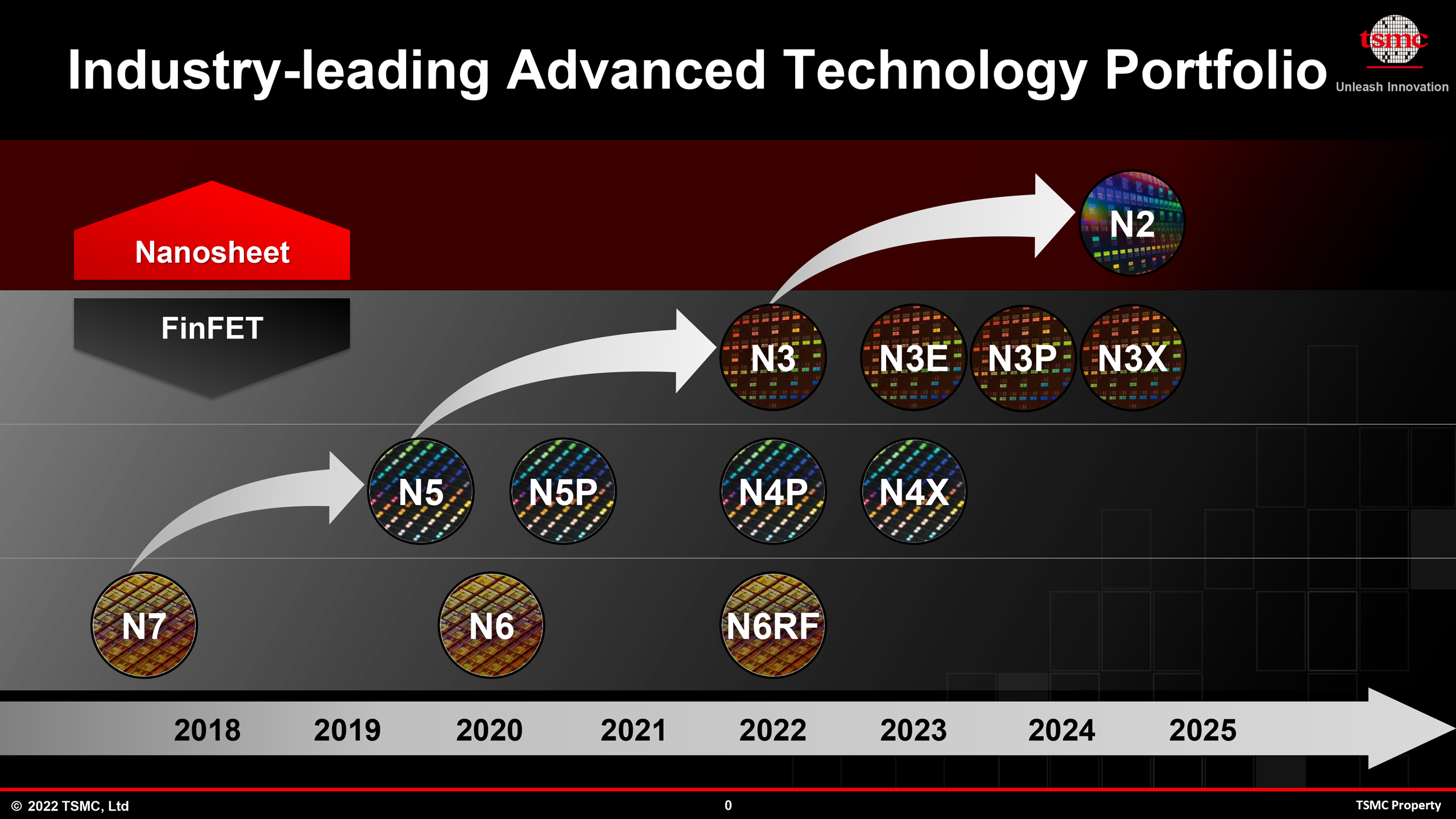
But, as it turns out, TSMC is not planning to start with both nanosheet GAA transistors and backside power rails in the initial generation of its N2 process technology. As disclosed by the company last week at their EU symposium, the first generation of N2 will only feature gate-all-around transistors. Backside power delivery, on the other hand, will come later with more advanced implementations of N2.
At this point the company hasn't said too much as to why they're not rolling out backside power delivery as part of their initial N2 node. But, in discussing the bifurcation, TSMC has noted that backside power delivery will ultimately add additional process steps, which the company is seemingly looking to avoid on their first try with GAAFETs.
The lack of backside power delivery in the original version of the N2 fabrication technology perhaps explains rather moderate performance improvement of N2 when compared to N3E node. While for high-performance computing (CPUs, accelerators, etc.) a 10% to 15% performance improvement at the same power and complexity does not seem to be impressive, a 25% to 30% power drop at the same speed and complexity seems to be very good for mobile applications.
| Advertised PPA Improvements of New Process Technologies Data announced during conference calls, events, press briefings and press releases |
|||||
| TSMC | |||||
| N5 vs N7 |
N3 vs N5 |
N3E vs N5 |
N2 vs N3E |
||
| Power | -30% | -25-30% | -34% | -25-30% | |
| Performance | +15% | +10-15% | +18% | +10-15% | |
| Chip Density* | ? | ? | ~1.3X | >1.1X | |
| Volume Manufacturing |
Q2 2022 | H2 2022 | Q2/Q3 2023 | H2 2025 | |
*Chip density published by TSMC reflects 'mixed' chip density consisting of 50% logic, 30% SRAM, and 20% analog.
Considering that TSMC always offers multiple versions of its nodes, that TSMC has several variants planned for N2 is not all that surprising. Nonetheless, it is a bit odd to see that TSMC is taking a rather long road to backside power delivery.
Compared and contrasted to the competition, this will end up being a notable difference from how rival Intel is planning to handle their own GAAFET/backside power transition with the Intel 20A process. Intel intends to introduce its GAA RibbonFET transistors and PowerVia interconnects together in mid-2024 – going so far as to create an internal pseudo node just to focus on RibbonFET development. TSMC, on the other hand, is taking a more cautious approach to risks and innovations, one which potentially has TSMC moving at a slower pace, but is also an approach that has traditionally been a better fit for TSMC's need to deliver more constant and consistent updates to its fab offerings.
And while we're still a few years out, it will be interesting to see what this means for the competitiveness of TSMC's first-generation N2 node. Will a GAAFET process without backside power delivery be at a meaningful disadvantage? Per current schedules, we'll find out the answer to that in the second half of 2025, when TSMC's first N2 node is slated to enter high-volume manufacturing (HVM).


14 Comments
View All Comments
ishould - Wednesday, June 29, 2022 - link
Honestly I like TSMC's iterative approach. Much more reliable node enhancements, even if incremental, vs Intel's 10nm delaydelaydelay because they were aiming for too high a target.Khanan - Wednesday, June 29, 2022 - link
Yep, Intels aggressive approach already failed once and that’s why I trust TSMC approach more and think it is the better one. Semiconductor is a risky business anyway, no need to make it even more risky.name99 - Wednesday, June 29, 2022 - link
"Nonetheless, it is a bit odd to see that TSMC is taking a rather long road to backside power delivery."Only if you haven't noticed TSMC's pattern since forever!
TSMC is all about
(a) not promising more than they are sure they can deliver
(b) cautious steps, not huge leaps
Let's see Intel actually deliver on their "this time, really, we promise, we can deliver GAA and BPD in time and on budget, just you wait"...
There's something bizarre about the tone of this whole article. We all know the first customer for N2 will be Apple, and while Apple would surely love increased density, they'd be OK with lower power and a SoC for that year whose primary feature is lower energy (just like the A15/M2). So Apple is the primary customer for N2 as just GAA, then the next year Apple (and followers) get N2E with BPD and another 20% or whatever density reduction.
Something like:
2022 (A16) new micro-architecture, N3
2023 iterate (within much the same area), N3E
2024 iterate (probably larger area), N3E
2025 iterate (energy as primary concern, like A15) N2
2026 new micro-architecture, take advantage of density boost from BPD
Everyone's happy!
This is (once again) the huge advantage TSMC has by having so many customers with so many different requirements. At least some can get substantial value from just GAA and the power reductions, without the density improvements of BPD.
Intel seems to have learned nothing from the past, not even on the foundry side! Why go to the trouble of these "internal-only" nodes like i4 and GAA-only i20? If you take foundry seriously, why not open up these nodes to others? Is there no-one in the whole world but Intel who could see some value in a high-performance-cell only i4, or a GAA-only i20? I just don't get it. It's like half the company insists "we can be a full service foundry like TSMC, just look at our Tower offerings", while the other half of the company insists "being a foundry is so much hassle, cleaning up all the edges and corners for outsiders! let's just not bother"
Compare with, say, AMZ. Of COURSE cleaning up all the edges and corners to get everything on micro-services that could be sold to 3rd parties was a hassle. But AMZ went all in, and thus success. INTC still seems unwilling to ACTUALLY go all-in with foundry.
name99 - Wednesday, June 29, 2022 - link
A different aspect to TSMC's decision is to consider the next step:After just a generation or so of GAA we have a generation of forksheet transistors, then we get to CFET. The question is
- do we deliver CFET as a separate sliver wafer of Si mounted on an underlying sliver wafer?
- which is in turn mounted on an underlying wafer of BPD?
On the one hand, OMG!
On the other hand, if you bite the bullet and create a full infrastructure for handling and stacking these sliver wafers, you're in a pretty good position, going forward, for dense monolithic 3D fabrication...
Whereas if your BPD is a one-trick pony that doesn't materially advance this larger (ten+ year) strategy, that seems a lost opportunity.
xol - Wednesday, June 29, 2022 - link
I'd think there's more profit for Intel if the chips they produce are their chips, and not someone elses. The exception to this would be if they get a big process advantage over TSMC/Samsung and can charge through the roof to discerning customers ie Apple.Strongly suspect beyond that, the "we foundry too now" messaging stuff is mostly business politics. (and that they won't be completive price wise/have a ton of customers lining up)
xol - Wednesday, June 29, 2022 - link
typo [competitive not completive]Khanan - Wednesday, June 29, 2022 - link
I agree, Intel foundry is odd, they should open it up.Freeb!rd - Wednesday, June 29, 2022 - link
"Why go to the trouble of these "internal-only" nodes like i4 and GAA-only i20? If you take foundry seriously, why not open up these nodes to others?"It seems to me that it is doubtful Intel has the EUV machine CAPACITY to offer it to foundry partners and also have volume for its own needs, yields may also be an issue. They use it internally until they get yields and volumes up and then allow foundry customers access to it. It still looks to me they won't truly be able to "catch up" to TSMC until the end of the decade.
whatthe123 - Wednesday, June 29, 2022 - link
intel can't deliver those nodes because they're incomplete and don't have enough capacity. it's not rocket science, even if you're optimistic and assume intel has working next gen nodes, it doesn't mean they can deliver all of them at the volume necessary for foundry services.whats with illuminati like conspiracy theory's surrounding intel? they've yet to prove they can execute, people aren't going to jump in on their foundry services unless they're competitive or offer serious discounts, it's literally that simple.
dotjaz - Thursday, June 30, 2022 - link
"Is there no-one in the whole world but Intel who could see some value in a high-performance-cell only i4"What are they gonna do with it? There's absolutely no standard library for anything.