Intel's Return to DRAM: Haswell GT3e to Integrate 128MB eDRAM?
by Anand Lal Shimpi on April 23, 2013 11:58 AM EST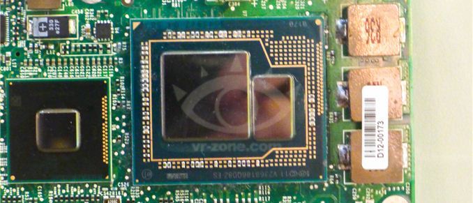
We've known for a while now that Intel will integrate some form of DRAM on-package for the absolute highest end GPU configurations of its upcoming Haswell SoC. Memory bandwidth is a very important enabler of GPU (and multi-core CPU) performance, but delivering enough of it typically required very high speed interfaces (read: high power) and/or very wide interfaces (read: large die areas). Neither of the traditional approaches to scaling memory bandwidth are low power or cost effective, which have kept them out of ultra mobile and integrated processor graphics.
The days of simple performance scaling by throwing more transistors at a design are quickly coming to an end. Moore's Law will continue but much like the reality check building low power silicon gave us a while ago, building high performance silicon will need some out of the box thinking going forward.
Dating back to Ivy Bridge (3rd gen Core/2012), Intel had plans to integrate some amount of DRAM onto the package in order to drive the performance of its processor graphics. Embedding DRAM onto the package adds cost and heat, and allegedly Paul Otellini wasn't willing to greenlight the production of a part that only Apple would use so it was canned. With Haswell, DRAM is back on the menu and this time it's actually going to come out. We've referred to the Haswell part with embedded DRAM as Haswell GT3e. The GT3 refers to the GPU configuration (40 EUs), while the lowercase e denotes embedded DRAM. Haswell GT3e will only be available in a BGA package (soldered-on, not socketed), and is only expected to appear alongside higher TDP (read: not Ultrabook) parts. The embedded DRAM will increase the thermal load of the SoC, although it shouldn't be as painful as including a discrete GPU + high speed DRAM. Intel's performance target for Haswell GT3e is NVIDIA's GeForce GT 650M.
What we don't know about GT3e is the type, size and speed of memory that Intel will integrate. Our old friend David Kanter at RealWorldTech presented a good thesis on the answers to those questions. Based on some sound logic and digging through the list of papers to be presented at the 2013 VLSI Technology Symposium in Kyoto, Kanter believes that the title of this soon to be presented Intel paper tells us everything we need to know:
"A 22nm High Performance Embedded DRAM SoC Technology Featuring Tri-Gate Transistors and MIMCAP COB"
According to Kanter's deductions (and somewhat validated by our own sources), Haswell GT3e should come equipped with 128MB of eDRAM connected to the main SoC via a 512-bit bus. Using eDRAM vs. commodity DDR3 makes sense as the former is easier to integrate into Intel's current fabs. There are also power, manufacturability and cost concerns as well that resulted in the creation of Intel's own DRAM design. The interface width is a bit suspect as that would require a fair amount of area at the edges of the Haswell die, but the main takeaway is that we're dealing with a parallel interface. Kanter estimates the bandwidth at roughly 64GB/s, not anywhere near high-end dGPU class but in the realm of what you can expect from a performance mainstream mobile GPU. At 22nm, Intel's eDRAM achieves a density of around 17.5Mbit/mm^2, which works out to be ~60mm^2 for the eDRAM itself. Add in any additional interface logic and Kanter estimates the total die area for the eDRAM component to be around 70 - 80mm^2. Intel is rumored to be charging $50 for the eDRAM adder on top of GT3, which would deliver very good margins for Intel. It's a sneaky play that allows Intel to capture more of the total system BoM (Bill of Materials) that would normally go to a discrete GPU company like NVIDIA, all while increasing utilization of their fabs. NVIDIA will still likely offer better perfoming solutions, not to mention the benefits of much stronger developer relations and a longer history of driver optimization. This is just the beginning however.
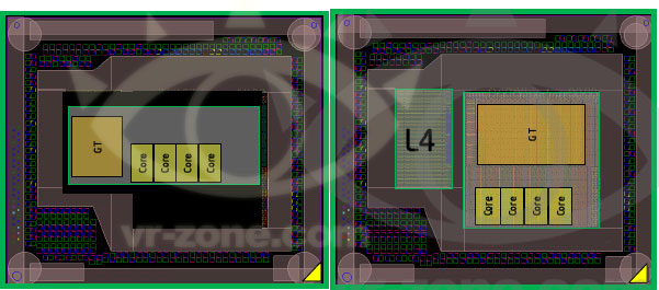
Based on leaked documents, the embedded DRAM will act as a 4th level cache and should work to improve both CPU and GPU performance. In server environments, I can see embedded DRAM acting as a real boon to multi-core performance. The obvious fit in the client space is to improve GPU performance in games. At only 128MB I wouldn't expect high-end dGPU levels of performance, but we should see a substantial improvement compared to traditional processor graphics. Long term you can expect Intel to bring eDRAM into other designs. There's an obvious fit with its mobile SoCs, although there we're likely talking about something another 12 - 24 months out.
AMD is expected to integrate a GDDR5 memory controller in its future APUs, similar to what it has done with the PlayStation 4 SoC, as its attempt to solve the memory bandwidth problem for processor based graphics.
Source: RealWorldTech


83 Comments
View All Comments
tipoo - Tuesday, April 23, 2013 - link
Also a unified fast memory between the GPU and CPU is exactly what is needed for good GPGPU performance, up until now the bottleneck was transferring things from the GPU memory to the CPU memory.Quizzical - Tuesday, April 23, 2013 - link
While this could conceivably have some big benefits for certain GPGPU applications, I really doubt that's the primary intended purpose. If you want to do serious GPGPU, you get a desktop or workstation or server or some such so that you can dissipate serious amounts of heat. You definitely don't get a laptop with dinky little integrated graphics that sports a peak GFLOPS rating of not much, which is the only place that GT3e is going to be used.Zandros - Tuesday, April 23, 2013 - link
IIIRC, compositing window managers provide a draw buffer for every open window, even if it's (partially) hidden. With a couple of windows open, that's easily tens of megabytes. Is there any reason to not keep those in the eDRAM?name99 - Saturday, April 27, 2013 - link
It's a way to make the research into eDRAM pay for itself while it goes on.It's essentially a research chip in this iteration. This means
(a) if they can't deliver, no catastrophe
(b) if the power utilization is higher than the actual benefits for general use cases, again no catastrophe.
I see the fact that they have gone this route rather than giving all the CPUs eDRAM as telling us that eDRAM is actually harder to get right than it looks, and they are being cautious. One might confirm this by noting that AMD has not jumped on eDRAM as a way to goose their sales, even though it would have been an obvious point of differentiation from Intel.
tynopik - Tuesday, April 23, 2013 - link
could it boot say XP without any additional memory added?marc1000 - Tuesday, April 23, 2013 - link
lol it would be awesome!tipoo - Tuesday, April 23, 2013 - link
This eDRAM could fit all of Windows 95 into it, imagine how fast that would be!tipoo - Tuesday, April 23, 2013 - link
Given how often it's repeated that Apple pushed for the eDRAM and higher performing integrated graphics in general, it seems like the classes the GT3e is put into miss the product it would benefit most, namely the 13" Macbook Pro and Retina version in particular. It seems only quad core 50+ watt TDP processors will get GT3e, and only ultrabooks will get GT3 without the eDRAM, so 13" laptops seem like they're stuck with GT2. A 15" laptop would generally have enough room for a better dedicated graphics chip, so it seems like it's missing what would be a perfect match for it.extide - Tuesday, April 23, 2013 - link
Where does it say that? It seems to me like GT3e will be available in the non ultrabok (read >17W TDP) chips, which mean the 35w class stuff they use in the 13" MBPr will have GT3e available.tipoo - Tuesday, April 23, 2013 - link
http://techreport.com/news/24564/leaked-slides-rev...Everything with 5200 (GT3e) is in the 47W range.