Testing Samsung 850 Pro Endurance & Measuring V-NAND Die Size
by Kristian Vättö on July 7, 2014 1:20 PM EST
Last week Samsung announced the 850 Pro, which is the first mainstream SSD to utilize 3D V-NAND. We already reviewed the drive and covered the fundamentals of V-NAND in detail but there is one thing I did not have the time to test: endurance. The most promising aspect of V-NAND is its increased endurance and Samsung has claimed endurance of up to ten times of 2D NAND. However, the 850 Pro is only rated at 150TB, which is twice the rating of 840 Pro, so I wanted to dig deeper and determine the endurance rating in terms of program/erase cycles.
To calculate the P/E cycles, I used a method similar to what we used with the SSD 840 two years ago. Basically, I wrote 128KB sequential data (QD1) to the drive and wrote down the necessary SMART values as well as the average throughput after every test. After repeating the test over a dozen times, I had enough data to figure out the P/E cycle count.
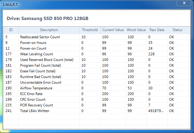
The Wear Leveling Count (WLC) SMART value gives us all the data we need. The current value stands for the remaining endurance of the drive in percentage, meaning that it starts from 100 and decreases linearly as the drive is written to. The raw WLC value counts the consumed P/E cycles, so if these two values are monitored while writing to the drive, sooner than later we will find the spot where the normalized value drops by one.
I found that the current WLC value drops by one after 60 P/E cycles (I ran the test over multiple WLC drops), which suggests that the WLC will drop to zero after 6,000 P/E cycles. In other words, the V-NAND in 850 Pro is good for 6,000 P/E cycles, which is twice the cycle count of modern 2D MLC NAND but quite far away from Samsung's "ten times the endurance" claims. Either Samsung is using lower binned parts in the 850 Pro (i.e. saving the 30,000 P/E cycle parts for enterprise drives) or the WLC value has artificially been limited to ensure that enterprises do not use the 850 Pro and pay the premium for the 845DC EVO/Pro instead. I am thinking it is more of the latter because the enterprise drives bring home much higher profits and of course Samsung wants to make sure that the 850 Pro is not used outside the client environment.
Once WLC reaches zero or one, it is generally a good idea to replace the drive as it may no longer be reliable. However, that does not mean that the drive will immediately fail -- according to JEDEC spec the P/E cycle rating is with one-year data retention, meaning that there can still be plenty of life left. The Tech Report's endurance testing gives a good picture of how much you can write after the WLC drops to zero, although personally I would still replace the drive ASAP because there is no guarantee that each drive performs similarly (remember, NAND is binned for endurance so there can be differences).
| SSD Lifetime Estimation | ||||
| 128GB | 256GB | 512GB | 1TB | |
| Raw NAND Capacity | 129GiB | 258GiB | 516GiB | 1032GiB |
| NAND P/E Cycles | 6,000 | |||
| Raw NAND Endurance | 755.9TiB | 1,511.7TiB | 3,023.4TiB | 6,046.9TiB |
| Lifespan with 20GiB of Host Writes per Day with 1.5x Write Amplification | 35.34 years | 70.68 years | 141.37 years | 282.74 years |
| Lifespan with 100GiB of Host Writes per Day with 3x Write Amplification | 7.07 years | 14.14 years | 28.27 years | 56.55 years |
| Drive Writes per Day with 5x Write Amplification | 1.10 | 1.10 | 1.10 | 1.10 |
The above table gives a good summary of how durable the 850 Pro really is. Even if you write 100GiB (GB in Windows is really GiB, i.e. 1024^3 bytes) per day with a write amplification of three, the smallest 128GB model will last for over seven years. 100GiB per day is very rare in a client environment and to be honest I can only see this applying to some high-end media professionals that use the drive for production purposes. On the other hand, media professionals will likely spring for a larger capacity anyway as 128GB might not even be capable of holding the data of one project. For a more typical user there is absolutely nothing to worry about as the 850 Pro will likely outlive the rest of the components.
Of course, there is still the 150TB write limitation on the warranty. That figure is based on host writes, so it applies even if you are only writing sequential data with low write amplification. Samsung did, however, tell me that they can make exceptions as long as the drive is used in client environment, meaning that the purpose of the endurance rating is mostly to make sure that the 850 Pro is not used in write intensive enterprise applications.
Testing Write Amplification
In addition to testing the endurance, I decided to see what the worst-case write amplification looks like. The test regime is similar to the endurance testing but the writes are 4KB random (QD32) to illustrate the worst possible scenario for the drive. Unfortunately, Samsung's SMART values do not report total NAND writes like Intel does, but the raw Wear Leveling Count basically gives us NAND writes in increments of the capacity of the drive (one P/E cycle = 129GiB of NAND writes for the 128GB drive). I recorded the Wear Leveling Count as well as the Total LBAs Written (i.e. host writes) value while writing 4KB random data to the drive.
| Worst-Case Write Amplification | |
| Host Writes | 493.9GiB |
| P/E Cycles Consumed | 42 |
| Approximate NAND Writes | 5,418GiB |
| Observed Write Amplification | 10.97x |
About 10x worst-case write amplification is fairly typical for a moden client SSD. Fortunately the days of +100x write amplification are over and under common client workloads the write amplification will usually stay below 2x.
| Worst-Case Endurance | ||||
| 128GB | 256GB | 512GB | 1TB | |
| Write Amplification | 11x | |||
| Total Bytes Written (TBW) | 68.7TiB | 137.4TiB | 274.9TiB | 549.7TiB |
| Drive Writes per Day for 5 Years | 0.43 | 0.43 | 0.43 | 0.43 |
The table above is just to show how the 850 Pro would bear in worst-case scenario that may be relevant to some enterprise users. I will be putting the 850 Pro through our enterprise test suite to see how it stacks up in terms of performance but especially with added over-provisioning, I can see the 850 Pro being viable for some read intensive enterprise workloads.


39 Comments
View All Comments
jjj - Monday, July 7, 2014 - link
You shouldn't assume that it makes sense from a cost perspective. Samsung is huge and sometimes it might focus less on cost ,maybe it's a commercial beta for now and they are not quite where they need to be.As for per layer you have 128Gb in 24 layers and 86Gb in 32 layers so a layer is 5.3333 Gb and 2.6875Gb and if you factor in die size the difference seems strangely high.
jjj - Monday, July 7, 2014 - link
Double posting here but just remembered,that i always wondered about temps for 3D NAND so , have you looked at heat and how it compares with 2D?Kristian Vättö - Monday, July 7, 2014 - link
Sure it's possible that Samsung is just "playing around with 32-layer design" but after all Samsung is a company with a target to generate profit for the shareholders. There must be a reason why Samsung didn't just add eight layers to the first Gen design and make it a ~170Gbit chip with about the same die size.Here are some numbers I crushed:
Die Size: 133mm^2 (1st gen) - 95.4mm^2 (2nd gen)
Observed Array Efficiency: 85% - 64%
Die Area Dedicated to Arrays: 113.1mm^2 - 61.1mm^2
Array Density: 1.13Gbit/mm^2 - 1.41Gbit/mm^2
Array Density per Layer: 0.047Gbit/mm^2 - 0.044Gbit/mm^2
In other words, when you take all the factors into account, it all adds up. Sure there is still a ~10% difference but nearly everything we have is estimations, so a 10% error sounds fair.
jjj - Monday, July 7, 2014 - link
Obviously smaller is most likely for yields reasons but it's not enough to draw the conclusion that cost per bit got better. I'm also not very sure how perf and power and heat changed from first gen to second, that's also a factor to consider when deciding to go this way.It is very likely that the first gen wasn't cost effective compared to 2D and all the other 3 big players are not jumping in just yet because of cost and that would suggest that for Samsung cost wasn't the main factor when they decided to launch 3D. As far as we can tell 3D is pretty low volume for now so the cost might matter very little for someone like Samsung. An objective could be to advance the technology while gaining share in enterprise SSD and enhancing the brand's image.
Second gen cost per bit could be better already or they could hope to get there soon but we just don't have the data to draw any conclusion.
jjj - Monday, July 7, 2014 - link
Looked at the numbers, i guess by looking at the area dedicated to the arrays there is only a small enough difference.Would be really nice to have some yield and cost projections based on die size, layers and process to try to figure out what the next steps will be.Second gen seems rather small given the array efficiency so maybe they'll aim for something bigger in gen 3. I am already dreaming of 140mm2 48 layer on 28nm at 512Gb at some point soon(ish).
repoman27 - Monday, July 7, 2014 - link
Some back of the envelope calculations show that the 2nd gen V-NAND would provide 6% fewer total bits per wafer, echoing your bit density calculations, but would come in the form of 40% more dies. If you expect even moderate issues with defects, that could make the 2nd gen much more profitable to produce, or simply a hedge as they ramp the number of layers with a relatively novel process.Samsung is pretty good at die stacking, but the other aspect may have to do with the smaller dies being much easier to stack in a standard 12 or 14 x 18mm package.
Per Hansson - Monday, July 7, 2014 - link
I'm having a hard time understanding the correlation of these numbers.A friend has a Intel X25-M G2 80GB drive that according to the SMART data has logged 73TB host writes.
That SSD has become slow, when testing using AS SSD it logs 1000ms on read access time for example.
Yet still the "media wearout indicator" is only at 97, implying the SSD has only used up 3% of it's life.
However the drive is warranted by Intel at a maximum of 7.5TB, so how do these numbers relate?
extide - Tuesday, July 8, 2014 - link
Speed and age have nothing to do with each otherextide - Tuesday, July 8, 2014 - link
Well, not nothing, but little enough that it is essentially nothing. The speed difference you are seeing are due to fragmentation at various levels. A secure erase would restore the drive to like-new speed.Per Hansson - Tuesday, July 8, 2014 - link
Thank you so much extide for your insight!I created a Ghost backup of the drive and did a secure erase (took a while to find a computer where hdderase.exe would work, and which would release the security frozen lock)
But once I did and restored the Ghost the drive is almost like new, write performance more than doubled and read access time went from ~1000ms to ~180ms
I also found another interesting thing out and that was by upgrading Intel SSD Toolbox from v3.1.6 to v3.2.1 the value "E1 Host Writes" went from 73TB down to 7.57TB (None of the other SMART values changed)
The Windows Experience Index score also went from 5.9 > 7.7
So far this SSD has 4.5 years of power on hours logged, so it's quite well used, only 96 power cycles, would be allot more without the UPS :)