iPhone 6s and iPhone 6s Plus Preliminary Results
by Joshua Ho on September 28, 2015 8:00 AM EST- Posted in
- Smartphones
- Apple
- Mobile
- PowerVR
- SoCs
- iPhone 6s
- iPhone 6s Plus
- Twister
At this point the iPhone release cycle is pretty well understood. One year, Apple releases the design refresh that changes the external design significantly while generally focusing on evolving the internal components. The year after, the S variant is released with the same design as the previous year, but with sweeping changes to the internals. This cycle of upgrades allows Apple to focus on updating one half of the iPhone at a time while essentially giving their teams a more comfortable two years to develop their next generation technologies.
The iPhone 6s fits into this model quite well, with the introduction of new features like 3D Touch and a 12MP camera that supports 4K video recording. However, it’s often difficult to understand exactly how much has changed with an S model as Apple tends to focus on high level features, this despite the fact that so many of the changes in an S model are at a low level. While I haven’t had a lot of time with the iPhone 6s yet, I wanted to share some of the first results that I’ve acquired over the course of testing the iPhone 6s and 6s Plus in the past few days.
The first, and probably biggest change that I haven’t seen addressed anywhere else yet is the storage solution of the iPhone 6s. Previous writers on the site have often spoken of Apple’s custom NAND controllers for storage in the iPhone, but I didn’t really understand what this really meant. In the case of the iPhone 6s, it seems that this means Apple has effectively taken their Macbook SSD controller and adapted it for use in a smartphone. Doing some digging through system files reveals that the storage solution identifies itself as APPLE SSD AP0128K, while the Macbook we reviewed had an SSD that identified itself as AP0256H.
While the name alone isn’t all that interesting, what is interesting is how this SSD enumerated. One notable difference is that this storage solution uses PCI-E rather than SDIO, so it’s unlikely that this is eMMC. Given the power requirements, it’s likely that this isn’t the same PCI-E as what you’d see in a laptop or desktop, but PCI-E over a MIPI M-PHY physical layer. By comparison, UFS's physical layer is MIPI M-PHY as well, while the protocol is SCSI. In essence, MIPI M-PHY is just a standard that defines the physical characteristics for transmitting signal, but SCSI and PCI-E are ways of determining what to do with that channel.
The iPhone 6s in turn appears to use NVMe, which rules out both UFS and traditional eMMC. To my knowledge, there’s no publicly available mobile storage solution that uses PCI-E and NVMe, so this controller seems to have more in common with the Macbook SSD controller than anything in the mobile space. It doesn’t seem this is an uncommon idea though, as SanDisk detailed the potential advantages of PCIE and NVMe in mobile storage at the Flash Memory Summit a month ago.
| NVMe | eMMC | |
| Latency | 2.8 µs | N/A |
| Maximum Queue Depth | Up to 64K queues with 64K commands each |
Up to 1 queue with 32 commands each |
| Duplex (Typical) | Full | Half |
The controller is a critical part of any storage component, but without any NAND to control it’s a bit pointless. Fortunately, the NAND used appears to be exposed in the OS as it’s referred to as 1Y128G-TLC-2P. Breaking this down, the 1Y means that we’re looking at 1Ynm NAND process with TLC. The TLC portion might concern some, but as we’ll soon see it turns out that we’re looking at a hybrid SLC/TLC NAND solution similar to SanDisk’s iNAND 7232 eMMC and desktop SSDs like Samsung’s 850 EVO which is better suited to the bursty workloads seen in mobile and PC segments. Between the 128GB and 64GB units we currently have, the 64GB unit uses Hynix NAND, but it remains to be seen who is supplying the NAND for the 128GB variants and what other suppliers exist for the 64GB SKUs.
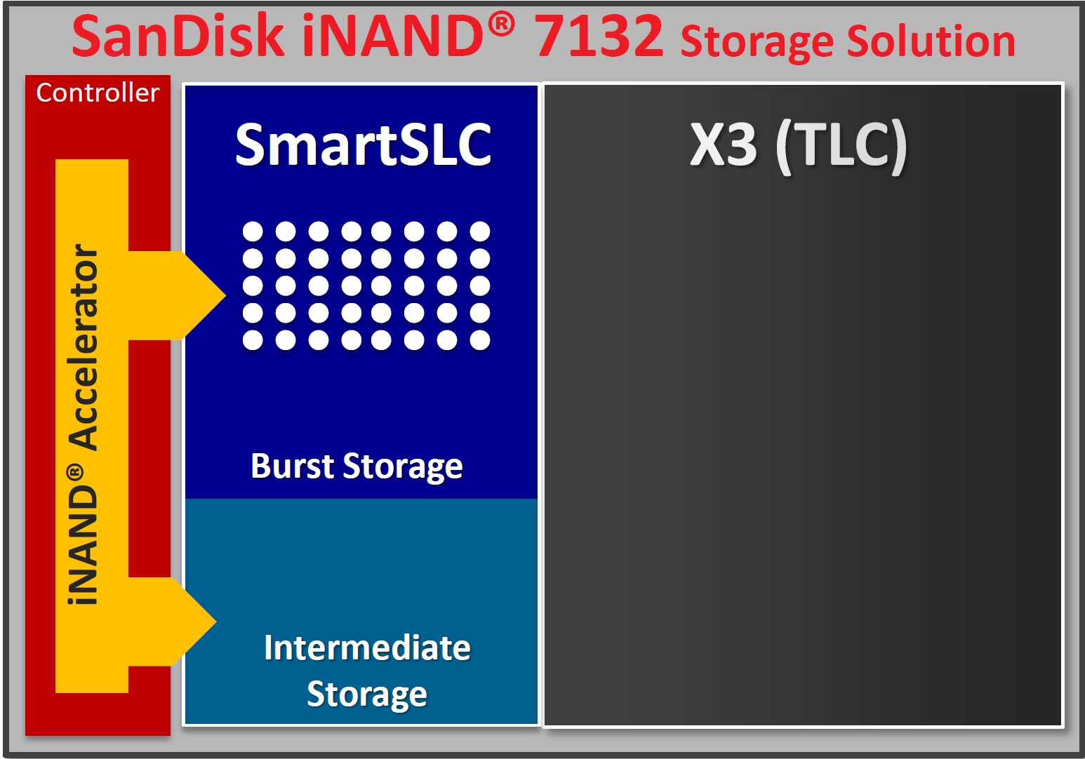
An example of how an SLC/TLC NAND storage device looks in mobile devices
For those that are unfamiliar how these hybrid SLC/TLC NAND solutions work, in essence the SLC cache is made sufficiently large to avoid showing the reduced performance of TLC NAND. Any time you’re writing to the storage, the writes go to the SLC cache first before being committed to TLC NAND. As long as the overall average bandwidth demand doesn’t exceed the speed of the TLC, short-run bandwidth is solely limited by the speed of the SLC cache, which turns out to be the case for almost every normal use case.
In order to see how all of this translates into performance, we once again use StorageBench, which is an app that allows us to do 256K sequential and 4K random storage performance testing developed by Eric Patno and is comparable to AndroBench 3.6.
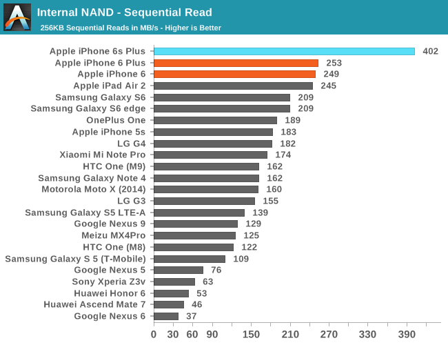
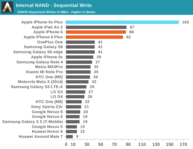
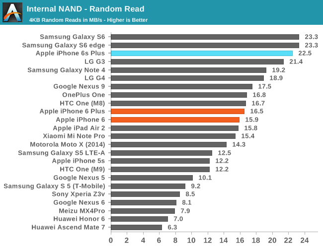
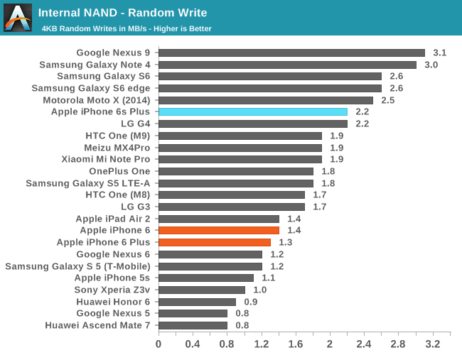
In practice, it seems random IO performance is relatively low, but it’s likely that we’re looking at a bottleneck of the testing methodology as the queue depth of the test is 1 and given PCB size limitations it isn’t reasonable to have as many NAND die working in parallel as we would see in something like a laptop. However, when we look at sequential speeds we can really start to see the strengths of the new storage controller and SLC/TLC. In the interest of seeing the limits of this SLC cache I decided to try running this test over a 5GB span.
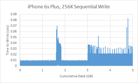
The graph is a bit difficult to interpret, but in effect we’re looking at the time it takes to write 256KB at a time until we get to 5GB. There are two notable spikes roughly around 2GB, but it appears to be small and likely to be some kind of garbage collection or some background work. At 3GB or so the latency increases which suggests that the SLC cache is overrun and write bandwidth is limited by TLC NAND performance.
Overall, NAND performance is impressive, especially in sequential cases. Apple has integrated a mobile storage solution that I haven’t seen in any other device yet, and the results suggest that they’re ahead of just about every other OEM in the industry here by a significant amount.
Storage aside, the SoC itself sees major changes this year. Apple has moved to a FinFET process from either TSMC or Samsung for the A9 SoC. However, it still isn’t clear whether the A9 is single source from one foundry or if A9 is being dual-sourced. Chipworks has reason to believe their iPhone 6s' A9 is fabricated on Samsung's 14nm process, though it hasn't been confirmed yet. Dual-sourcing is well within Apple's capabilities, however TSMC's 16nm and Samsung's 14nm process are not identical - naming aside, different processes developed by different fabs will have different characteristics - so dual-sourcing requires a lot more work to get consistent chips out of both sources. For what it's worth A8 was initially rumored to be dual-sourced as well, but decapping by Chipworks only ever turned up TSMC chips.
Update: Chipworks has since taken apart multiple phones and confirmed that Apple is indeed dual-sourcing; both Samsung and TSMC are supplying chips
Moving on, let's talk about initial performance and battery life measurements, which look promising. Of course, it’s worth noting that the web browser benchmarks we currently have are often optimization targets for OEMs, so web browser benchmarks seen here aren’t necessarily evidence that the browser experience will be performant and smooth across all scenarios.
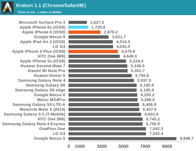
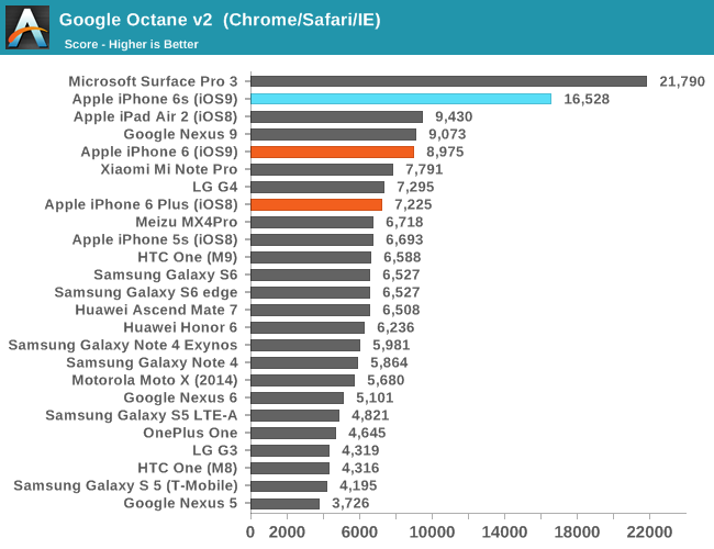
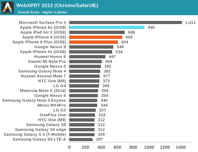
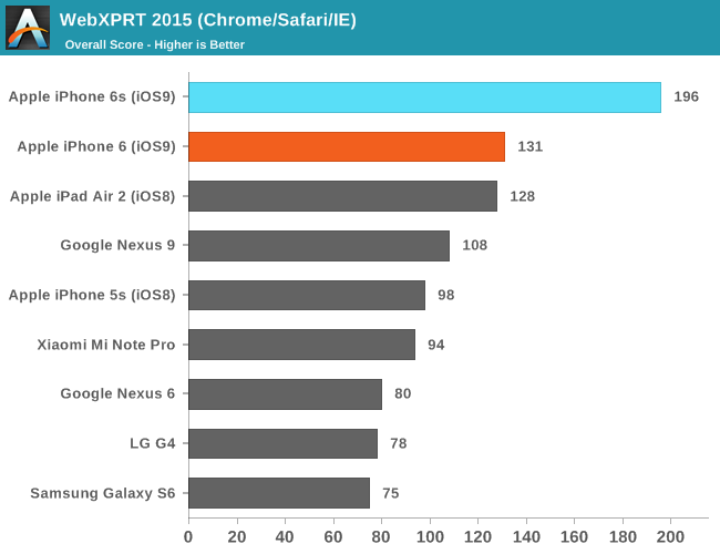
Regardless of whether an OEM is optimizing specifically for these benchmarks, it’s hard to ignore just how well Apple has optimized Safari and the dual core Twister CPUs as they’ve effectively set new records for these benchmarks in mobile. Of course, to try and really figure out the relative performance between CPU architectures when ignoring differences in operating system and developer convention we’ll have to turn to some of our native benchmarks such as SPEC CPU2000, but this will have to wait for the full review. What we can look at are some of our standard benchmarks that test graphics and game-related performance.
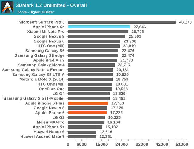
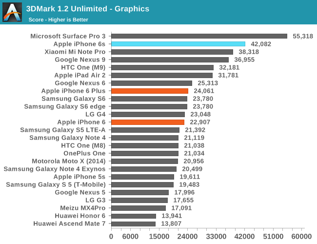
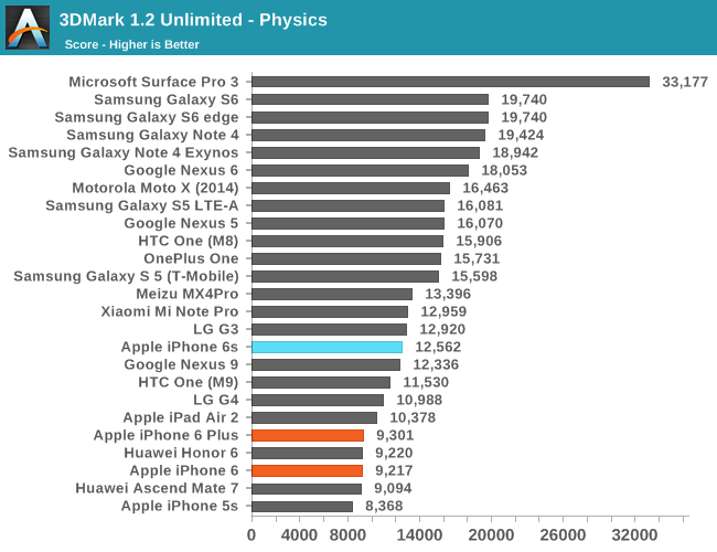
In 3DMark, we see the continuation of a long-running trend in the physics test in which the primary determinant of performance is clock speed and memory performance as data dependencies mean that much of the CPU’s out of order execution assets go unused. However, in graphics we see an enormous improvement, to the extent that the A9’s PowerVR GPU is actually beating the iPad Air’s GXA6850 GPU by a significant margin.
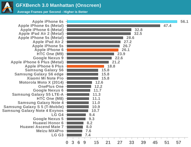
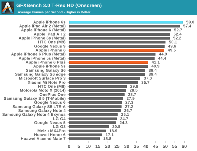
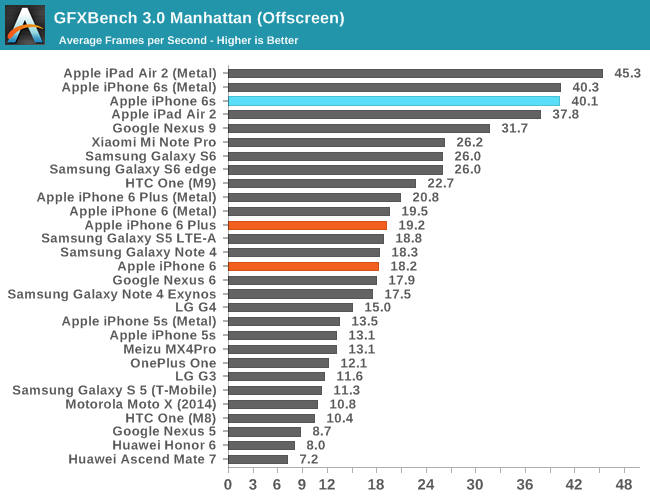
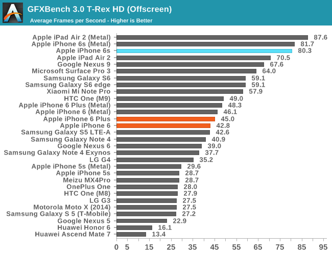
In GFXBench, we see a similar trend which is incredible to think about. Apple has managed to fit a GPU into the iPhone 6s that is more powerful than what was in the iPad Air 2 for OpenGL ES, which is really only possible because of the new process technology that enables much lower power consumption and higher performance.
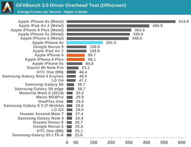
While I don’t normally call attention to most of the GFXBench subtests, in this case I think the driver overhead is worthy of special attention as it highlights one of the real-world benefits that improved CPU performance has. While we often think of CPU and GPU performance as orthogonal, the GPU is fundamentally tied to CPU performance to a certain extent as traditional APIs like OpenGL ES can have significant CPU overhead, especially as GPU performance has grown far faster than CPU performance. For APIs like OpenGL ES, to set up a frame it’s necessary for the CPU to check that the API call is valid, then do any necessary GPU shader or state compilation and begin running code on the GPU at draw time, which incurs increasing overhead as scenes become more complex. Through a combination of efficient drivers and enormous CPU performance, the dual core Twister CPU manages to set a new record for OpenGL ES driver overhead.
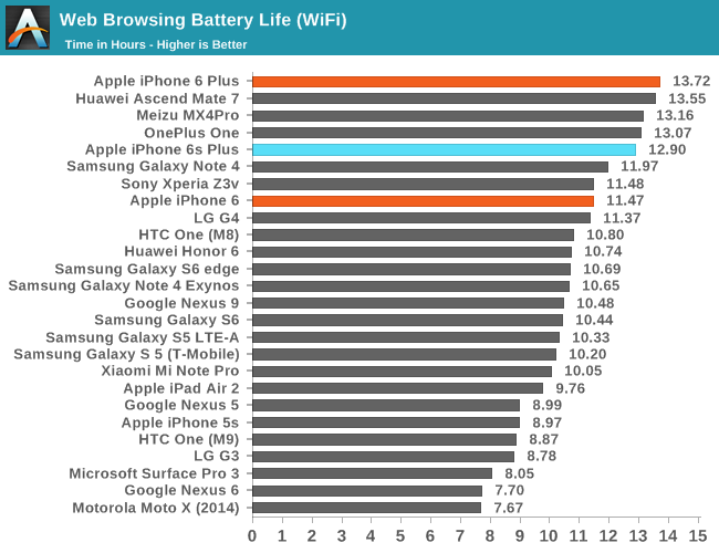
The final piece of data I've been able to collect over the course of the past few days is basic WiFi battery life. For those that are unfamiliar with the changes from the iPhone 6 line to iPhone 6s, the iPhone 6s now has a 1715 mAh (6.517 WHr) battery, and the iPhone 6s Plus has a 2750 mAh (10.45 WHr) battery. Both have a battery about 5.5-6% smaller than the previous generation.
Interestingly, the iPhone 6s Plus appears to actually have accordingly less battery life at 12.9 hours, or right around 6% less than the iPhone 6 Plus. This could be evidence that there haven't been any efficiency improvements to the iPhone 6s line, but given that our testing shows Apple is already at the point where our web browsing test is effectively a pure display rundown it's likely we're looking at the worst-case difference. This warrants additional investigation, but it's possible that a more balanced workload will even out the difference in battery life and maybe even tilt the scales back towards the iPhone 6s depending upon how much load is placed on the SoC.
Overall, while there’s still a great deal of work left to do to exhaustively evaluate the iPhone 6s and 6s Plus, the initial results are quite positive. I haven’t finished a detailed investigation into the architecture of Twister, but I suspect we’re looking at some pretty significant changes compared to Typhoon, which would be unlike the smaller move from Cyclone to Typhoon. The GPU improvements are enormous, and while we don’t have enough data to determine whether the iPhone 6s retains the same sustained GPU performance that we saw in the iPhone 6, the peak performance figures are impressive to say the least. The SSD-like storage solution is also a major surprise, and likely to be overlooked as its effects are often hard to distinguish without direct comparison. Battery life does regress in a single test, but I suspect in real-world situations with less of a focus on the display battery life will either be equal or favor the iPhone 6s, so it will be interesting to see if Apple's battery life estimates remain as accurate as they traditionally have been. We’ve definitely discovered much more about the iPhone 6s than what we’re able to cover in this initial article, so stay tuned for the full review.


185 Comments
View All Comments
Gondalf - Monday, September 28, 2015 - link
But no :). This SOC has 8MB of L3 and 3MB of L2, so it is all data and code caching with these short benchmarks suited for SOCs with relatively little caches.The real world usage will be a lot slower, moreover likely all this is not sustained like is happened with A7.
After all it is only a 3W SOC there isn't a single chance it is two or three times faster of 7420 3W too and done on the same process.
Samsung and Qualcomm are pretty quiet trust me, there is a lot of benchmark optimization in this device. The gigantic caches are there to fake all the phone cpu benches.
Tech_guy - Monday, September 28, 2015 - link
The performance and smoothness in games I get on my iPhone 6(yes the 6) vs my girl friend's S6 makes a strong case that these benchmarks are NOT inflated or faked. I totally believe these as truth, the 6s is the faster device. I mean how can you even argue 2500 single core geekbench vs 1450 single core on the 7420. That can't be "faked" Geekbench is a neutral test they don't care, it's totally based on HOW FAST the cpu's actually can complete the tests.Gondalf - Monday, September 28, 2015 - link
You ""believe"" firmly, still you don't read the posts of other writers.My point is about the massive caching (9MB of cache) that gives massive advantages on very small phone benches. Do you have undestood??
And no Geek is not neutral, it has massive issues as the cache grow up.
name99 - Monday, September 28, 2015 - link
IF your claims were true --- that all it takes to make a fast low-power CPU is to dump 9MB (don't know where you get that number from -- it's 8MiB L3 and 3MiB L2) of cache on the die, then why didn't Apple do that last year, or the year before? Hell what's to stop Samsung doing it now?Morawka - Monday, September 28, 2015 - link
That L3 8MB is actually the SRAM which is used by fingerprint device and other devices.. The L2 is what the cpu and gpu have dedicated access to.name99 - Monday, September 28, 2015 - link
Some day, dude, you're going to look at this stage of your commenting on AnandTech and cringe...To give just one example:
Look at the graph at the bottom of this page:
http://www.anandtech.com/show/8554/the-iphone-6-re...
If the CPU has no access to the L3, what do you think that plateau between 1024 and 4096 refers to?
tuxRoller - Monday, September 28, 2015 - link
Why? Why would it need that?SRAM for that? Why? Trustzone (it had its own memory system) is used for this sort of thing and it's perfect for it.
An interrupt causes trustzone to take over, it handles the data and responds, one way or the other, with ios kernel never touching the data.
tipoo - Monday, September 28, 2015 - link
Not saying it's faked, I completely believe Apples single core performance lead, but since you mentioned GB specifically I think Anandtech had some qualms a while ago about discrepancies between the iOS and Android builds of it. Hardware decryption also throws a very large number into the averaging. That's why you may see ARM chips matching Core M, but then in something like Linpack the Core M is 8x faster.name99 - Monday, September 28, 2015 - link
The Geekbench3 workloads ARE smaller than their desktop workloads. This is true; the sizes of the data sets for each workload are available at www.primatelabs.com/geekbench3/workloads.pdf.This is because (in the past) the cores were slow enough that using full workloads would have taken forever. BUT
(a) John Poole says he has run the full workloads on various mobile cores and in all it makes less than 1% difference.
(b) Geekbench 4 will come out soonish, and will use identical workloads for mobile and desktop. John has said nothing about this, but I'm guessing it doesn't change the ratings much between x86 and various ARMs --- if it did he'd be preparing the way, I suspect, warning people not to take Geekbench 3 too serious anymore.
(c) These devices ARE running real world code --- what do you think browsers are --- and the performance numbers behave in pretty much the same way for all the benchmarks.
Morawka - Monday, September 28, 2015 - link
because on the geekbench benchmark, it is never writing to main memory on the 6S, it's using fast cache all the time.. I agree, the cache sizes are making this soc look waaay better than it actually is. in real world usage, your app is gonna use way more than 8MB of that cache, therefore requiring access to main memory.