So went the review of the original 5AGM from Chaintech, an AT Socket-7 AGP motherboard that brought more than a well written manual to the buying scene. Now, three months later, armed with the VIA MVP3 chipset, can Chaintech find a worthy successor to their hit board in the 5AGM2? Or have times changed so incredibly much that a worthy successor to the original 5AGM just won't cut it? In the slowly maturing Super7 world, let's see how well the 5AGM2 stacks up against its older brother, and more importantly, the competition.
Anand Tech Report Card Rating
95/A
| CPU Interface | Socket-7 |
| Chipset | VIA MVP3 |
| L2 Cache | 512KB |
| Form Factor | AT (w/ AT & ATX PS Connectors) |
| Bus Speeds | 60 / 66 / 75 / 83 / 100 MHz |
| Clock Multipliers | 1.5x - 5.5x |
| Voltages Supported | 2.2v / 2.8v / 2.9v / 3.2v / 3.3v / 3.5v |
| Memory Slots | 3 168pin DIMM Slots (EDO/SDRAM) |
| Expansion Slots | 1 AGP Slot 3 PCI Slots (1 Full Length) 3 ISA Slots (1 Shared / 2 Full Length) |
| BIOS | AWARD PnP BIOS |
| A 90 degree rotation of the CPU Socket, the removal of all SIMM slots, and the addition of a third DIMM slot are what separate the Chaintech 5AGM2 from probably its most fierce competitor, the FIC VA-503+. Unlike some AT form factor Super7 motherboards, the 5AGM2 does give you the option of using a Voodoo2 based accelerator or any other full length PCI cards in the last of the three PCI slots the board is equipped with. The three complimentary ISA slots on the board are positioned in such a way that two are usable by full length cards, making room for your old sound card in your new purchase. Parallel to the peripheral expansion slots are your three DIMM slots, accepting either EDO or SDRAM DIMMs of any speed as long as they work at the 66MHz FSB frequency. | 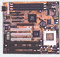 |
The heart of the 5AGM2 is the incredibly popular VIA MVP3 chipset, coupled with the 512KB of on-board L2 cache the chipset allows for a fairly sizable 128MB Cacheable Memory Area. The board AnandTech tested was using revision 'CD' of the chipset while you can expect all newer 5AGM2's to come prepared with the newest 'CE' revision which boasts full compatibility with i740 graphics accelerators. While the 5AGM2 tested didn't experience any problems with an i740 accelerator when the proper drivers and patches were applied from VIA (www.via.com.tw), this may not be true for all 'CD' based boards so to be on the safe side remember to check for a 'CE' revision label.
Setting up the 5AGM2 isn't as bad as the VA-503+ from FIC, however because of the more advanced chipset, the 5AGM2 is a bit more complicated than the original 5AGM as far as configuration and initial setup is concerned. The FSB settings, selectable from a list topping out at 100MHz and bottoming out at 60MHz, are controlled by three individual jumpers out of a block containing 7 total. Three more of the 7 jumpers make up the clock multiplier selection settings, offering possibilities in the 1.5x to 5.5x range. Voltage settings are controlled by a separate jumper block adjacent to the CPU Socket wedged between one of the 19 electrolytic capacitors spread throughout the board and a 3-pin CPU fan connector. The last jumper on the FSB/clock multiplier block allows you to select the memory bus frequency, you can either have it run at the FSB frequency or at your AGP Clock Frequency which is usually around 66MHz. Courtesy of the MVP3 chipset you can re-use your standard SDRAM or even EDO RAM as long as it is available in a 168-pin DIMM package and can cope with at least the speed of your AGP Bus. Considering the extremely affordable $84 price tag of the 5AGM2, this makes putting together a high-end system on a low-end budget within the reach of virtually anyone.
The jumper setup on the 5AGM2 is much easier than most motherboards in its class excluding the Epox MVP3C-M, as if that weren't enough, the classic 54-page User's Manual from Chaintech will make the 5AGM2 an experience you will definitely remember. From the Jumper Layout & Diagram quick reference sticker in the back of the manual, to the diagrams which populate the well written manual, Chaintech's intentions were made quite clear in the words printed on the box: "We Don't Imitate, We Innovate." Don't plan on finding any forms of corporate flattery in the Chaintech User's Manual, sticking to their slogan the manual imitates no other except in its quality. Also bundled with the 5AGM2 are the VIA Bus Master IDE drivers and the AGP Drivers for the MVP3 chipset, as a general rule of thumb, if you plan on using a DVD-ROM drive with your system you will want to avoid using the VIA drivers in favor of the Microsoft DMA drivers that come bundled with Windows 9x to avoid any problems.
Stability and performance are what can be expected from the majority of well made Super7 motherboards, overall, a decent product and a worthy successor to the 5AGM throne...but is that enough?
A common item left out of the bundles of most AT motherboards is a USB header to let you take advantage of a board's USB support, this common occurrence unfortunately is present with the 5AGM2. With USB devices becoming more commonplace among the average computer owner expect to spend around $10 - $20 on a USB header to take advantage of the MVP3 Chipset's USB support. Other than that, there isn't much more to complain about with the 5AGM2. Excellent price, outstanding written documentation, and a well made board make the 5AGM2 worthy of the Chaintech name.
Number of Universal Serial Bus Root Ports: 0
USB IRQ Enable/Disable in BIOS: Yes
USB Keyboard Support in BIOS: Yes
Chaintech 5AGM2 Chipset Features Setup |
||
| Item | Settings | |
| 66/75/83/100MHz FSB | Safe | |
| Bank 0/1 DRAM Timing: | 60/10 ns | 70/12 ns |
| Bank 2/3 DRAM Timing: | 60/10 ns | 70/12 ns |
| Bank 4/5 DRAM Timing: | 60/10 ns | 70/12 ns |
| SDRAM Cycle Length: | 2 | 3 |
| SDRAM Bank Interleave: | Enabled | Disabled |
| DRAM Read Pipeline: | Enabled | Disabled |
| Cache Strategy: | WT | WT |
| Cache Rd+CPU Wt Pipeline: | Enabled | Enabled |
| Read Around Write: | Enabled | Disabled |
| Cache Timing: | Fastest | Fast |
| Video BIOS Cacheable: | Enabled | Disabled |
| System BIOS Cacheable: | Enabled | Disabled |
| Memory Hole At 15Mb Addr.: | Disabled | Disabled |
| AGP: | Enabled | Enabled |
| Aperture Size: | 64M | 8M |
| AGP 2X-Mode: | Enabled | Disabled |
| Flash BIOS Protection: | Enabled | Disabled |
Note: Disable "Read Around Write" when using i740 based accelerators
Recommended SDRAM: AMM PC100 SDRAM, Azzo PC100
SDRAM, Corsair PC100 SDRAM; Memory Man PC100 SDRAM
SDRAM Tested: 1 x 64 AMM PC100 SDRAM, 1 x 64 Azzo PC100 SDRAM, 1 x 64MB Corsair PC100
SDRAM; 1 x 64MB Memory-Man PC100 SDRAM
Manufacturer: Advanced American Megatrends
Technologies
Purchase Web-Site: http://www.megacom.com
Manufacturer: Azzo Computers
Purchase Web-Site: http://www.azzo.com
Manufacturer: Corsair Microsystems
Purchase Web-Site: http://www.tccomputers.com/
Manufacturer: The Memory Man
Purchase Web-Site: http://www.memory-man.com


0 Comments
View All Comments