AMD Zen 2 Microarchitecture Analysis: Ryzen 3000 and EPYC Rome
by Dr. Ian Cutress on June 10, 2019 7:22 PM EST- Posted in
- CPUs
- AMD
- Ryzen
- EPYC
- Infinity Fabric
- PCIe 4.0
- Zen 2
- Rome
- Ryzen 3000
- Ryzen 3rd Gen
Windows Optimizations
One of the key points that have been a pain in the side of non-Intel processors using Windows has been the optimizations and scheduler arrangements in the operating system. We’ve seen in the past how Windows has not been kind to non-Intel microarchitecture layouts, such as AMD’s previous module design in Bulldozer, the Qualcomm hybrid CPU strategy with Windows on Snapdragon, and more recently with multi-die arrangements on Threadripper that introduce different memory latency domains into consumer computing.
Obviously AMD has a close relationship with Microsoft when it comes down to identifying a non-regular core topology with a processor, and the two companies work towards ensuring that thread and memory assignments, absent of program driven direction, attempt to make the most out of the system. With the May 10th update to Windows, some additional features have been put in place to get the most out of the upcoming Zen 2 microarchitecture and Ryzen 3000 silicon layouts.
The optimizations come on two fronts, both of which are reasonably easy to explain.
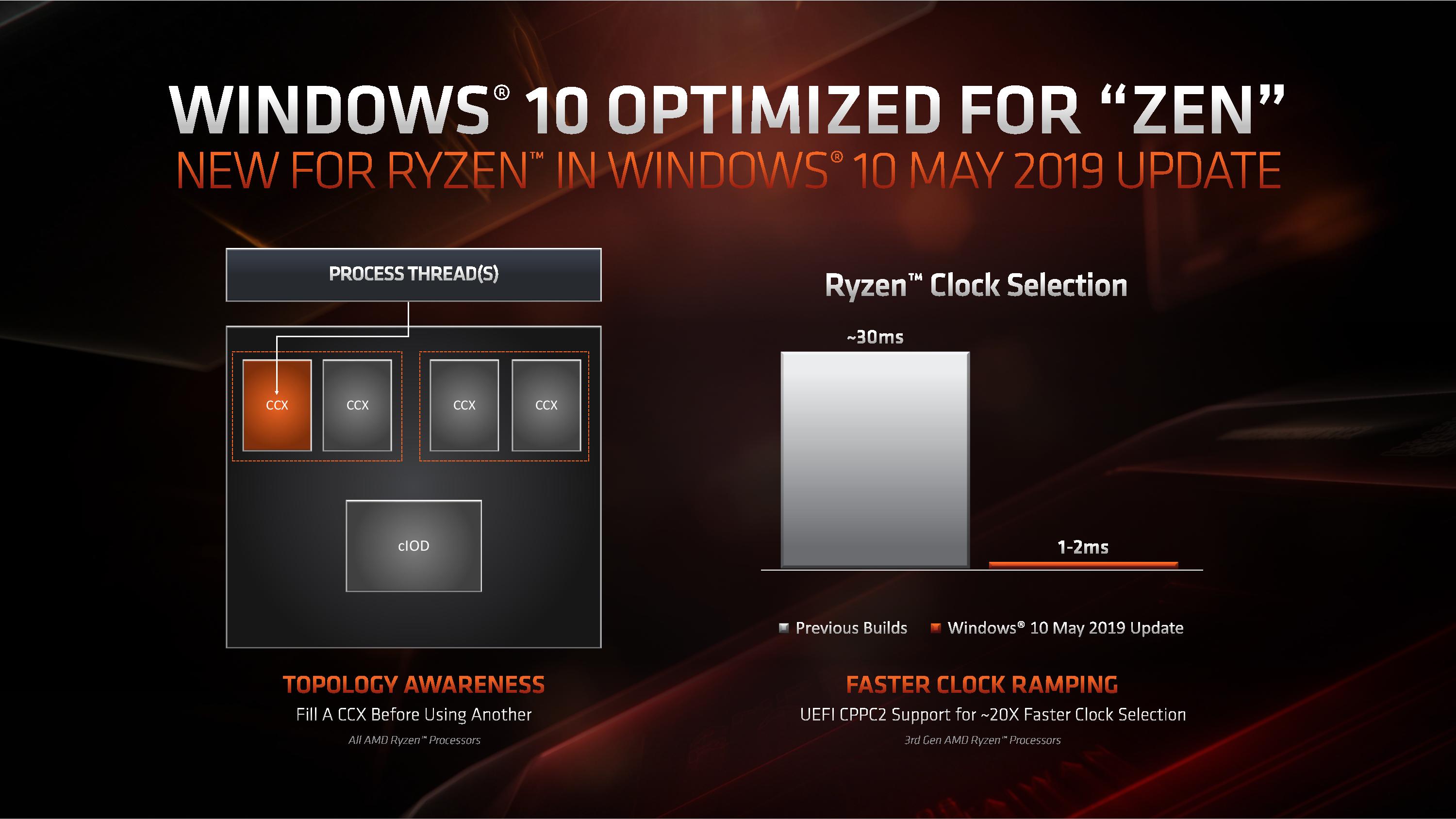
Thread Grouping
The first is thread allocation. When a processor has different ‘groups’ of CPU cores, there are different ways in which threads are allocated, all of which have pros and cons. The two extremes for thread allocation come down to thread grouping and thread expansion.
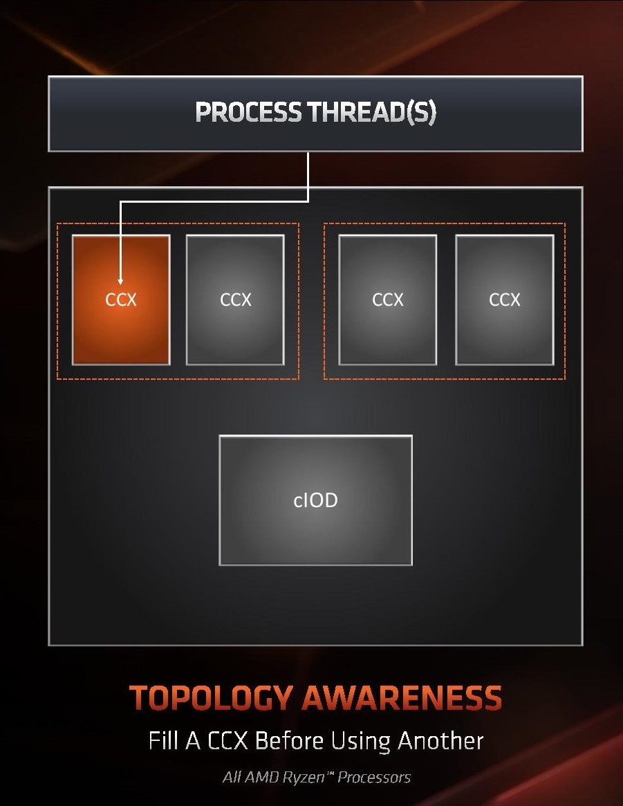
Thread grouping is where as new threads are spawned, they will be allocated onto cores directly next to cores that already have threads. This keeps the threads close together, for thread-to-thread communication, however it can create regions of high power density, especially when there are many cores on the processor but only a couple are active.
Thread expansion is where cores are placed as far away from each other as possible. In AMD’s case, this would mean a second thread spawning on a different chiplet, or a different core complex/CCX, as far away as possible. This allows the CPU to maintain high performance by not having regions of high power density, typically providing the best turbo performance across multiple threads.
The danger of thread expansion is when a program spawns two threads that end up on different sides of the CPU. In Threadripper, this could even mean that the second thread was on a part of the CPU that had a long memory latency, causing an imbalance in the potential performance between the two threads, even though the cores those threads were on would have been at the higher turbo frequency.
Because of how modern software, and in particular video games, are now spawning multiple threads rather than relying on a single thread, and those threads need to talk to each other, AMD is moving from a hybrid thread expansion technique to a thread grouping technique. This means that one CCX will fill up with threads before another CCX is even accessed. AMD believes that despite the potential for high power density within a chiplet, while the other might be inactive, is still worth it for overall performance.
For Matisse, this should afford a nice improvement for limited thread scenarios, and on the face of the technology, gaming. It will be interesting to see how much of an affect this has on the upcoming EPYC Rome CPUs or future Threadripper designs. The single benchmark AMD provided in its explanation was Rocket League at 1080p Low, which reported a +15% frame rate gain.
Clock Ramping
For any of our users familiar with our Skylake microarchitecture deep dive, you may remember that Intel introduced a new feature called Speed Shift that enabled the processor to adjust between different P-states more freely, as well as ramping from idle to load very quickly – from 100 ms to 40ms in the first version in Skylake, then down to 15 ms with Kaby Lake. It did this by handing P-state control back from the OS to the processor, which reacted based on instruction throughput and request. With Zen 2, AMD is now enabling the same feature.

AMD already has sufficiently more granularity in its frequency adjustments over Intel, allowing for 25 MHz differences rather than 100 MHz differences, however enabling a faster ramp-to-load frequency jump is going to help AMD when it comes to very burst-driven workloads, such as WebXPRT (Intel’s favorite for this sort of demonstration). According to AMD, the way that this has been implemented with Zen 2 will require BIOS updates as well as moving to the Windows May 10th update, but it will reduce frequency ramping from ~30 milliseconds on Zen to ~1-2 milliseconds on Zen 2. It should be noted that this is much faster than the numbers Intel tends to provide.
The technical name for AMD’s implementation involves CPPC2, or Collaborative Power Performance Control 2, and AMD’s metrics state that this can increase burst workloads and also application loading. AMD cites a +6% performance gain in application launch times using PCMark10’s app launch sub-test.
Hardened Security for Zen 2
Another aspect to Zen 2 is AMD’s approach to heightened security requirements of modern processors. As has been reported, a good number of the recent array of side channel exploits do not affect AMD processors, primarily because of how AMD manages its TLB buffers that have always required additional security checks before most of this became an issue. Nonetheless, for the issues to which AMD is vulnerable, it has implemented a full hardware-based security platform for them.
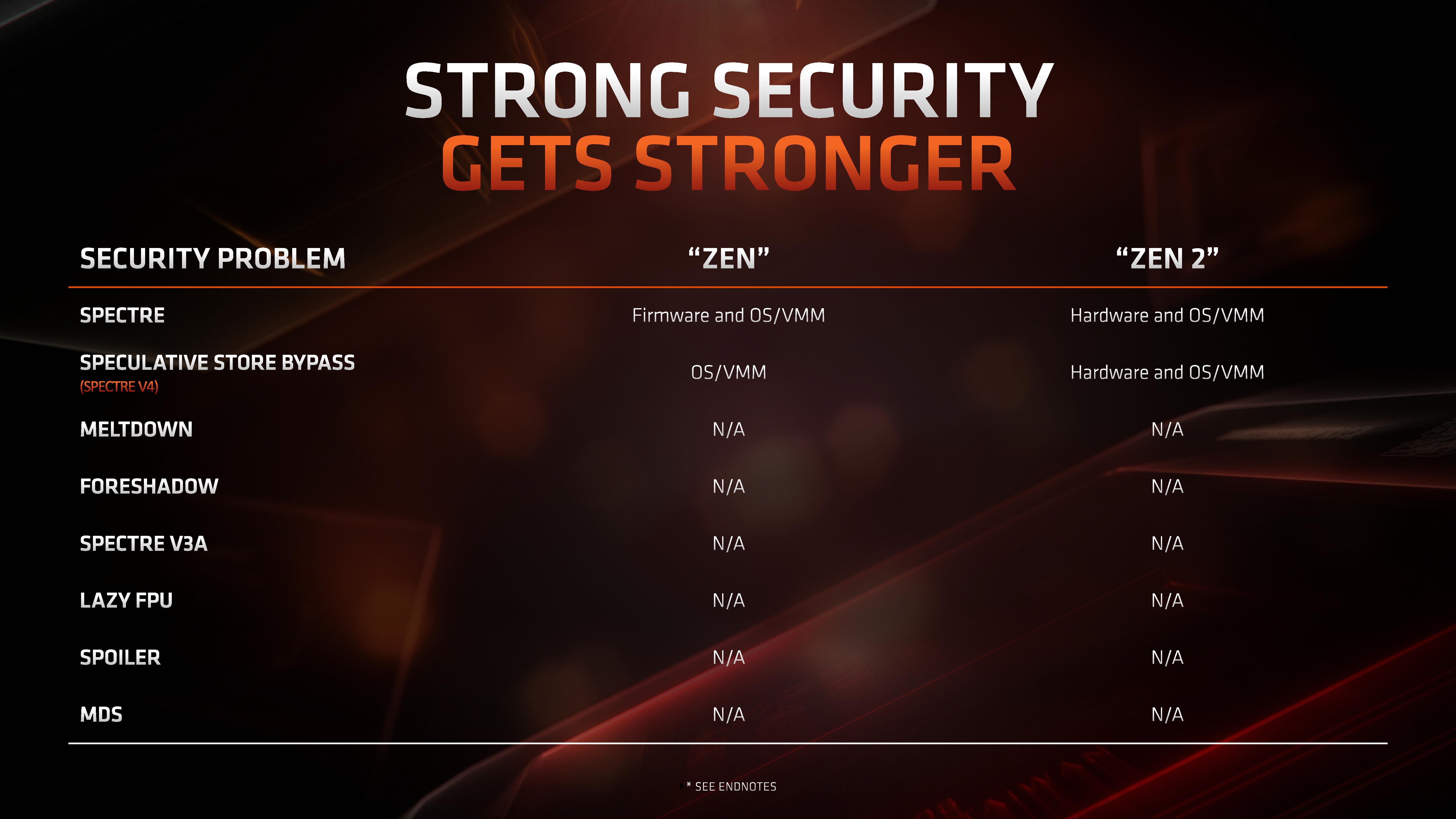
The change here comes for the Speculative Store Bypass, known as Spectre v4, which AMD now has additional hardware to work in conjunction with the OS or virtual memory managers such as hypervisors in order to control. AMD doesn’t expect any performance change from these updates. Newer issues such as Foreshadow and Zombieload do not affect AMD processors.


216 Comments
View All Comments
eek2121 - Wednesday, June 19, 2019 - link
I think what people are getting at is having an L4 Cache. Such a cache would be slower than L3, but would be much faster than DRAM (for now, DDR 5133 was recently demonstrated, that is 2566 MHz double data rate). HBM2 is a prime candidate for that because you can stick 8 Gb on a CPU for $60 and with some engineering work, it would help performance massively. 8 gb could hold practically everything needed in cache. That being said, there are engineering challenges to overcome and I doubt this will ever be a thing.Once JEDEC approves RAM running at DDR 5600 at reasonable timings it won’t matter anyway. AMD can simply bump up the IF speed to 1:1 and with shortened RAM traces, performance penalties can be minimized.
jamescox - Saturday, June 22, 2019 - link
For an interposer based Epyc package for the next generation, I would expect perhaps they do an active interposer with all of the external interface transistors in the interposer. They could do similar things with a passive interposer also though. The passive interposer could be an intermediate between Zen 3 and Zen 4. Then they could place a large number of 7 nm+ chiplets on the interposer. As I said, it is hard to speculate, but an option that I thought of based on AdoredTV 15 chiplet rumor would be to have 4 memory controller chips, each one running 2 channels (128-bit) DDR5. Those chips would just be the memory controller logic if on an active interposer and the interfaces to the interposer connections. That isn’t much so at 7 nm and below, they could place massive L4 SRAM caches on the memory controller chips. Current ~75 square mm Zen 2 chiplets have 16 MB plus 8 cpu cores, so it could be a large amount of cache; perhaps something like 64 or 128 MB per chip. It wouldn’t be a cheap device, but AMD’s goal is to get into the high end market eventually.The other chiplets could be 1 or two die to manage connections out to the cpu chiplets. This would just be the logic with an active interposer. With a regular interposer, it would need to have the IO transistors also, but the interfaces are quite small. A single infinity fabric switch chip handling all cpu chiplets could provide very low latency. They may have another chip with a switch to tie everything together or they could actually place a couple cpu chiplets on the interposer. Two extra cpu chiplets or one 16 core chiplet could be where the 80 core rumor came from. A possible reason to do that is to allow an HBM based gpu to be mounted on either side. That would make an exceptional HPC product with 16 cores (possible 64 threads if they go to 4 way SMT) and 2 HBM gpus. Another way to get 80 core would be to just make a 3 CCX chiplet with 12 cores. It looks like the Epyc package will not fit all 12 core die though. A mixture of 4 12-core and 4 8-core looks like it would fit, but it wouldn’t be symmetric though. That would allow a quick Zen 2+ style upgrade. Desktop might be able to go to 24 cores and Epyc to 80. The confusion could be mixing up a Zen 2+ rumor and a Zen 3 rumor or something like that. The interposer makes a lot of sense for the giant IO die that cannot be easily implemented at 7 nm. The yields probably don’t support that large of die, so you use an interposer and make a bunch of 100 square mm sized die instead.
I can’t rule out placing HBM on an IO interposer, but due to the latency not really being that much better than off package DRAM, especially at DDR5 speeds, it just doesn’t seem like they would do it.
nandnandnand - Sunday, July 7, 2019 - link
"That being said, there are engineering challenges to overcome and I doubt this will ever be a thing."Putting large amounts of DRAM ever closer to the CPU will definitely be a thing:
https://www.darpa.mil/attachments/3DSoCProposersDa...
Intel is already moving in this direction with Foveros, and AMD is also working on it:
https://www.tomshardware.com/news/amd-3d-memory-st...
It doesn't matter how fast DDR5 is. The industry must move in this direction to grab performance and power efficiency gains.
AdrianMel - Sunday, June 16, 2019 - link
I would like these AMD chips to be used on laptops. It would be a breakthrough in computing power, low consumption. I think that if a HBM2 memory or a larger memory is integrated into the processor, I think it will double the computing power. It would be a study and implementation of 2 super ports, the old expresscard 54 in which we can insert 2 video cards in laptopsnandnandnand - Sunday, July 7, 2019 - link
AMD needs to put out some 6-8 core Zen 2 laptop chips.peevee - Monday, June 17, 2019 - link
Does it mean that AVX2 performance doubles compared to Zen+? At least on workloads where data for the inner loop fits into L1D$ (hierarchical dense matrix multiplication etc)?peevee - Monday, June 17, 2019 - link
"AMD manages its L3 by sharing a 16MB block per CCX, rather than enabling access to any L3 from any core."Does it mean that for code and shared data caches, 64MB L3 on Ryzen 9 behaves essentially like 16MB cache (say, all 12/16 cores run the same code as it usually is in performance-critical client code and not 4+ different processes/VMs in parallel)? What a waste it is/would be...
jamescox - Saturday, June 22, 2019 - link
The caches on different CCXs can communicate with each other. In Zen 2, those one the same die probably communicate at core clock rather than at memory clock; there is no memory clock on the cpu chiplet. The speeds between chiplets have essentially more than doubled the clocks vs. Zen 1 and there is a possibility that they doubled the widths also. There just about isn’t any way to scale to such core counts otherwise.An intel monolithic high core count device will have trouble competing. The latency of their mesh network will go up with more cores and it will burn a lot of power. The latency of the L3 with a mesh network will be higher than the latency within a 4-core CCX. Problems with the CCX architecture are mostly due to OS scheduler issues and badly written multithreaded code. Many applications performed significantly better on Linux compared to windows due to this.
The mesh network is also not workable across multiple chiplets. A 16-core (or even a 10 core) monolithic device would be quite large for 10 nm. They would be wasting a bunch of expensive 10 nm capacity on IO. With the large die size and questionable yields, it will be a much more expensive chip than AMD’s MCM. Also, current Intel chips top out at 38.5 MB of L3 cache on 14 nm. Those are mostly expensive Xeon processors. AMD will have a 32 MB part for $200 and a 64 MB part for $500. Even when Intel actually gets a 10 nm part on the desktop, it will likely be much more expensive. They are also going to have serious problems getting their 10 nm parts up to competitive clock speeds with the 14 nm parts. They have been tweaking 14 nm for something like 5+ years now. Pushing the clock on their problematic 10 nm process doesn’t sound promising.
peevee - Monday, June 17, 2019 - link
"One of the features of IF2 is that the clock has been decoupled from the main DRAM clock....For Zen 2, AMD has introduced ratios to the IF2, enabling a 1:1 normal ratio or a 2:1 ratio that reduces the IF2 clock in half."
I have news for you - 2:1 is still COUPLED. False advertisement in the slides.
And besides, who in their right mind would want to halve IF clock to go from DDR3200 to even DDR4000 (with requisite higher timings)?
BMNify - Saturday, June 22, 2019 - link
the only real world test that matters in the UHD2/8K Rec. 2020/BT.2020 LIVE NHK/bbc broadast of the 2020 Summer Olympics will begin on Friday, 24 July and related video streams is can AMD Zen 2 do it can any pc core do realtime x264/x265/ffmpeg software encoding and x264/x265 compliant decoding (notice how many hw assisted encoders today dont decode to spec as seen when you re-enode them with the latest ffmpeg), how many 8k encodes and what overheads are remaining if any can even do one...