Intel’s 11th Gen Core Tiger Lake SoC Detailed: SuperFin, Willow Cove and Xe-LP
by Dr. Ian Cutress on August 13, 2020 9:01 AM EST- Posted in
- CPUs
- Intel
- SoCs
- Tiger Lake
- 10+
- Xe-LP
- Willow Cove
- Intel Arch Day 2020
- SuperFin
- 10SF
What is Xe-LP?
A big part of the Tiger Lake/Ice Lake comparison will be the performance difference in graphics. Where Ice Lake has 64 Execution Units of Gen11 graphics, Tiger Lake has 96 Execution Units but of the new Xe-LP architecture. On top of that, there’s the new SuperFin transistor stack that promises to drive frequencies (and power windows) a lot higher, making Tiger Lake more scalable than before.
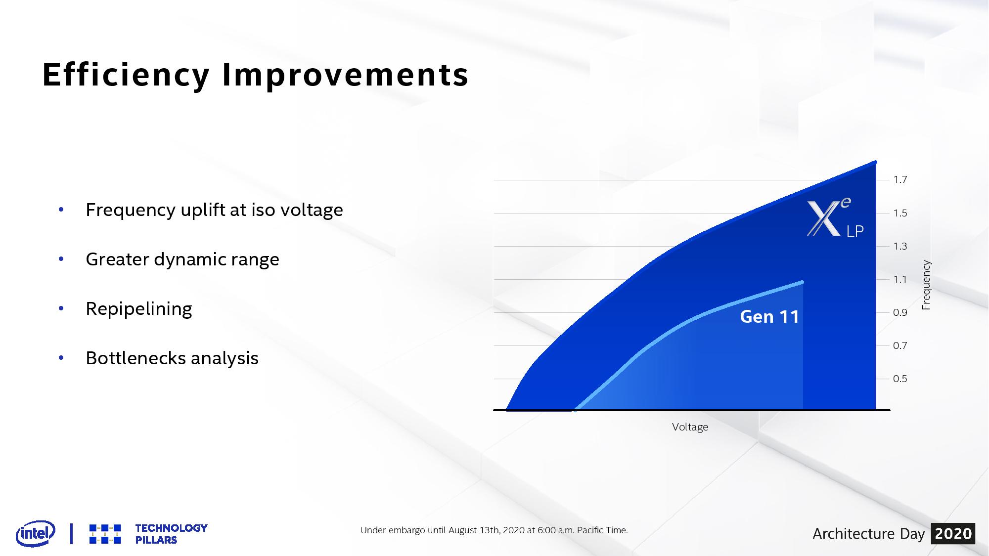
Straight off the bat Intel’s graphs are showing that at the same voltage, where Ice Lake Gen11 achieves 1100 MHz, the new Xe-LP graphics will get to ~1650 MHz, a raw +50% increase. That means at Ice Lake’s peak power, we should expect Tiger Lake to perform at a minimum 2.25x better. Expanding beyond that, the peak for Tiger Lake seems to be in the 1800 MHz range, ultimately giving a minimum 2.45x more performance over Ice Lake. This is before we even start talking about the fundamental differences in the Xe-LP architecture compared to Gen11.
Intel is promoting Xe-LP as operating at 2x the performance of Gen11, so even though these numbers might easily suggest a 2.25x uplift before taking into account the architecture, it will ultimately depend on how the graphics is used.
Gen11 vs Xe-LP
For a more in-depth look into Intel’s Xe graphics portfolio, including HP, HPC, and the new gaming architecture HPG, Ryan has written an article covering Xe in greater detail. In this article, we’ll cover the basics.
In the Ice Lake Gen11 graphics system, each one of the 64 execution units consisted of two four-wide ALUs, one set of four for FP/INT, and the other set of four for FP/Extended Math. 16 of these execution units would form a sub-slide within Gen11.
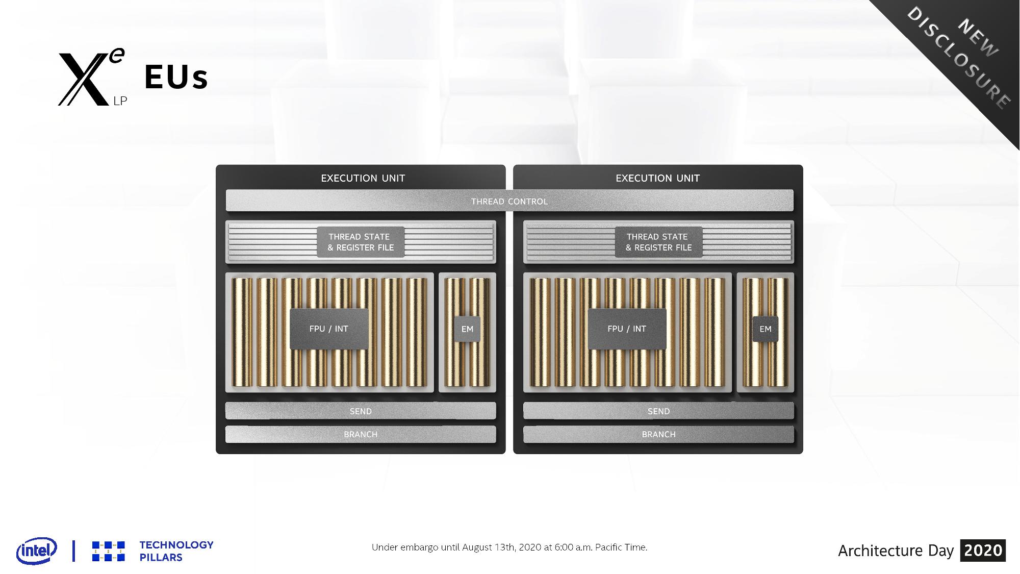
For Xe-LP, that 4+4 per execution unit has been rebalanced for this target market. There are now 10 ALUs per execution unit, but in an 8+2 configuration. The 8 ALUs support 2xINT16 and INT32 data types, but also with new DP4a instructions can accelerate INT8 inference workloads. The new execution units also now work in pairs – two EUs will share a single thread control block to help assist with coordinated workload dispatch.
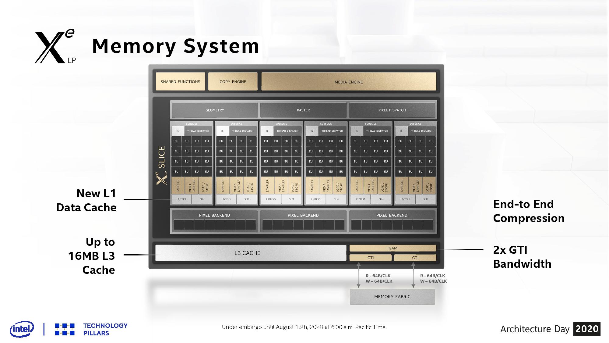
As with ICL, 16 of the EUs now form a sub-slice with the graphics, and slices are added in the SoC as performance is needed. What is new in Tiger Lake is that each sub-slice now has its own L1 data and texture cache, and the pixel backend runs 8 pixels/clock per two sub-slices.
Overall the graphics system can support 1536 FLOP/clock, with the samplers at 48 Tex/clock per sub-slice and a total of 24 pixel/clock in the back-end. LP in Tiger Lake has 16 MiB of its own L3 cache, separate from the rest of the L3 cache in the chip, and the interface to the memory fabric is doubled, supporting 2x64B/clock reads or writes or a combination of both.
Exact performance numbers for Xe-LP in Tiger Lake are going to be a question mark until we get closer to launch. Intel has stated that the discrete graphics version of LP, known as DG1, is due out later this year.
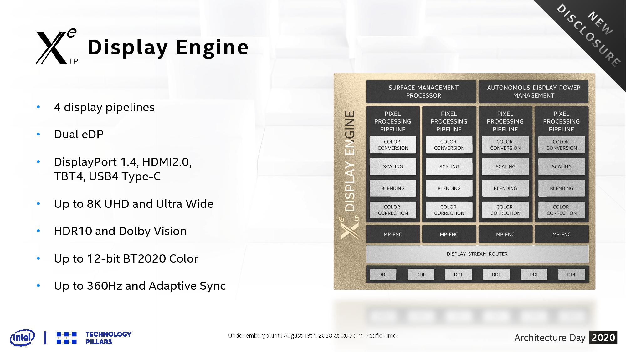
Xe-LP Media and Display
The other question on Tiger Lake on graphics will be the media and display support. Tiger Lake will be Intel’s first official support for the AV1 codec in decode mode, and Intel has also doubled its encode/decode throughput for other popular codecs. This means a full hardware-based 12-bit video pipeline for HDR and 8K60 playback support.
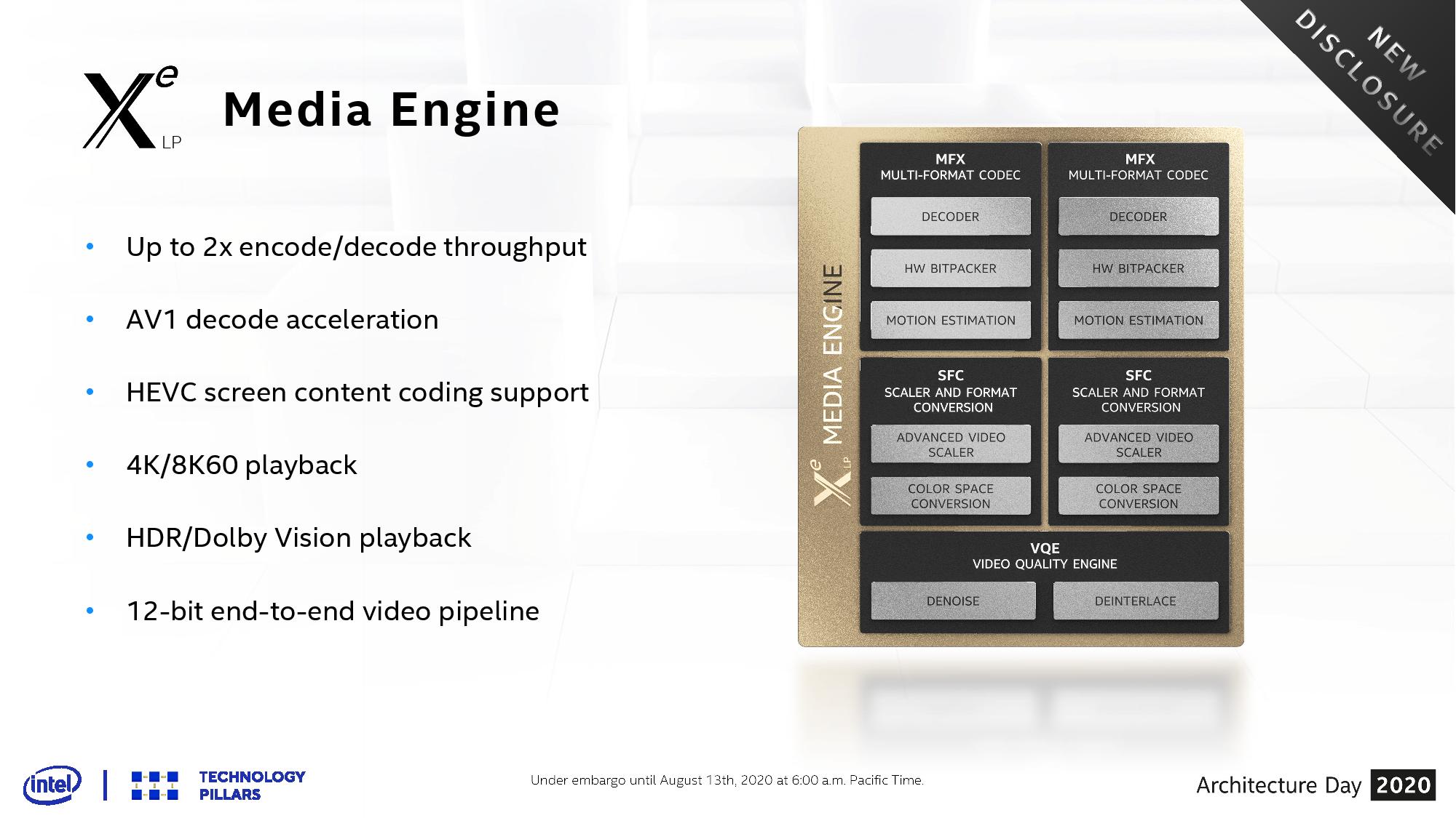
Display Support for Tiger Lake is also extended with four 4K display pipelines. Connections over DP1.4, HDMI 2.0, Thunderbolt 4, and USB4 Type-C simultaneously is how Intel expects users to operate if all four outputs are needed at once. The display engine also supports HDR10, 12-bit BT2020 color, Adaptive Sync, and support for monitors up to 360 Hz.
External Graphics and Hybrid Support
One of the interesting questions we posted to Intel during Architecture Day was surrounding how Xe-LP will operate in the presence of additional graphics, and potentially paired with a discrete version of LP later in the year. Unfortunately there seemed to be some confusion between the definitions of ‘hybrid’ graphics vs ‘switchable’ graphics, so we got that cleared up in time for the article.
At present, Intel expects almost all Tiger Lake solutions to run in devices where there is no discrete graphics solution – only the integrated graphics is provided as the primary compute for gaming and acceleration. However, Tiger Lake will support switchable graphics solutions with Xe-LP discrete graphics. Intel did not state if this was discrete graphics with respect to a built LP chip or an external discrete graphics solution through Thunderbolt.
Due to Tiger Lake’s PCIe 4.0 support and Thunderbolt 4 support, depending on how an exact Tiger Lake system is configured, Intel expects that any discrete graphics solution will operate at a lower latency, mostly due to the fact that the PCIe 4.0 lanes will be directly attached to the CPU, rather than a chipset. Intel quoted ~100 nanosecond lower latency. They also stated an 8 GB/s bandwidth to main memory, which seemed a bit low?
On the topic of hybrid graphics, where the integrated graphics and an Xe-LP discrete solution could work in tandem on the same rendering task, Intel stated that there is no plan to support a Multi-GPU solution of this configuration.


71 Comments
View All Comments
Fr@nk - Saturday, August 15, 2020 - link
A socketed TGL 8c/16t would destroy the incoming Rocket Lake so I very doubt Intel will release the TGL 8c for retail desktop consumer. Maybe for OEM-only, just like desktop Renoirballsystemlord - Saturday, August 15, 2020 - link
Spelling and grammar errors:This means that the new cores in Tiger Lake a built that for any given power or voltage, they will run at a higher frequency.
That made no sense. I have no suggestions on how to improve it.
After Ice Lake was set to be Tiger Lake, built on a '10+' manufacturing node.
It's a bit confusing as worded. Try an extra ",":
After, Ice Lake was set to be Tiger Lake, built on a '10+' manufacturing node.
"At a high level this means that if a laptop is playing a video, on the CPU we have the display engine is on and the video decode on,"
Excess "is":
"At a high level this means that if a laptop is playing a video, on the CPU we have the display engine on and the video decode on,"
attaran - Saturday, August 15, 2020 - link
Missing Bloomfield that came before er Lynnfield & Clarksfield and used the same process.xtess3ractx - Sunday, August 16, 2020 - link
What I want to know is where are the desktop 10nm big core parts? where are they? seriously? you're telling me you cant make 10nm octa core? seriously?10nm with ddr4 and ddr5, pcie 4, thunderbolt, get it done, otherwise im finally switching to amd how long must i wait.
Meteor2 - Tuesday, August 18, 2020 - link
Why haven't you switched already? Everyone else has. Look at the sales charts.AbRASiON - Monday, August 17, 2020 - link
Well when will we see a 15w 'lite' version (4 core, no HT) version as a "tiger lake celeron" or "tiger lake pentium" in an Intel NUC?Sounds like a nice mobile chip
Spunjji - Monday, August 17, 2020 - link
Small error on page 1, start of the 6th paragraph:"Intel first unveiled its Core microarchitecture in Q1 2006, as an offshoot of the more power efficient Pentium Pro products" - It was an offshoot of the Pentium M (although that does of course owe a lot to the P6 architecture).
Spunjji - Monday, August 17, 2020 - link
That Core family chart on the first page is good for a chuckle.Conroe - _Core 2_ - is apparently now the first generation of Core. 🤪
It beggared belief enough when they gave Lynnfield that title after the release of Sandy Bridge, but it seems we're deep into revising the revisionism now?
Nehalem and Westmere are now part of the same "first generation" as Conroe, despite the fact that they marked two major steps in integration for Intel - first with the PCH on-die, and then with the GPU on-package.
Meanwhile Skylake and its *extremely minor derivatives* span *four whole generations*, while poor little Palm Cove / Cannon Lake just wasn't any sort of generation at all. It all seems to painfully arbitrary.
In case there was any doubt left after all these decades: Intel is primarily a marketing company.
xpclient - Monday, August 17, 2020 - link
So it will be a while before on-chip AV1 encoding arrivesMeteor2 - Tuesday, August 18, 2020 - link
Yes that's my take-away, which is frustrating