Intel's Process Roadmap to 2025: with 4nm, 3nm, 20A and 18A?!
by Dr. Ian Cutress on July 26, 2021 5:00 PM ESTIntel’s Next Generation Packaging: EMIB and Foveros
Alongside the process node advancements, Intel also has to march forward with next-generation packaging technology. The demand for high performance silicon coupled with increasingly difficult process node development has created an environment where processors are no longer a single piece of silicon, relying on multiple smaller (and potentially optimized) chiplets or tiles to be packaged together in a way that benefits performance, power, and the end product.
Single large chips are no longer the smart business decision – they can end up too difficult to make without defects, or the technology to create them isn’t optimized for any one particular feature on the chip. However, dividing a processor up into separate silicon pieces creates additional barriers to moving data around between those pieces – if the data has to transition from being in silicon to being in something else (such as a package or an interposer) then there is a power cost and latency cost to consider. The tradeoff is optimized silicon built for purpose, such as a logic chip made on a logic process, a memory chip made on a memory process, and the smaller chips often have better voltage/frequency characteristics when binning than their larger counterparts. But underpinning all of this is how the chips are put together, and that requires packaging.
Intel’s two main specialist packaging technologies are EMIB and Foveros. Intel explained the future of both in relation to its future node development.
EMIB: Embedded Multi-Die Interconnect Bridge
Intel’s EMIB technology is designed for chip-to-chip connections when laid out on a 2D plane.
The easiest way for two chips on the same substrate to talk to each other is by taking a datapath through the substrate. The substrate is a printed circuit board made of layers of insulated material interspersed with metal layers etched into tracks and traces. Depending on the quality of the substrate, the physical protocol, and the standard being used, it costs a lot of power to transmit data through the substrate, and bandwidth is reduced. But, this is the cheapest option.
The alternative to a substrate is to put both chips onto an interposer. An interposer is a large piece of silicon, big enough for both chips to wholly fit on to, and the chips are bonded directly to the interposer. Similarly there are data paths put into the interposer, but because the data is being moved from silicon to silicon, the loss of power is not as much as a substrate, and the bandwidth can be higher. The downside to this is that the interposer also has to be manufactured (usually on 65nm), the chips involved have to be small enough to fit, and it can be rather expensive. But, the interposer is a good solution, and active interposers (with built in logic for networking) have yet to be fully exploited).
Intel’s EMIB solution is a combination of both interposer and substrate. Rather than taking a large interposer, Intel uses a small slither of silicon and embeds that directly into the substrate, and Intel calls this a bridge. The bridge is effectively two halves with hundreds or thousands of connections each side, and the chips are built to connect to one half of the bridge. Now both chips are connected to that bridge, having the benefit of transferring data through silicon without the restrictions that a large interposer might bring. Intel can embed multiple bridges between two chips if more bandwidth is needed, or multiple bridges for designs using more than two chips. Also, the cost of that bridge is much less than a large interposer.
First Generation EMIB
With those explanations, it sounds like Intel’s EMIB is a win-win. There have been a few limitations to the technology – actually embedding a bridge into a substrate is kind of hard. Intel has spent several years and lots of money trying to perfect the technology for low power operation. On top of this, whenever you are adding multiple elements together, there is an associated yield with that process – even if connecting a chip to a bridge has a 99% yield, doing it with a dozen chips on a single design reduces the overall yield down to 87%, even when starting with known good chips (that have their own yield). When you hear that Intel has been working on bringing this technology to volume, it is these numbers they are trying to improve.
Intel currently has EMIB in the market on several of its products, most noticeably its Stratix FPGA and Agilex FPGA families, but it was also part of its Kaby G line of mobile processors, connecting a Radeon GPU to high-bandwidth memory. Intel has already stated that it is coming to several future products, such as Ponte Vecchio (supercomputer-class graphics), Sapphire Rapids (next generation Xeon enterprise processor), Meteor Lake (2023 consumer processor), and others related to graphics.

Intel's Ponte Vecchio uses EMIB and Foveros
On the roadmap side of EMIB, Intel is reducing the bump pitch over the next few years. When the chips are connected to the bridges embedded in the substrate, they connect across bumps, and the distance between the bumps is known as the pitch – the smaller the bump pitch, the more connections can be made in the same area. This allows the chip to either increase bandwidth, or reduce the bridge size. The first generation EMIB technologies in 2017 were using 55 micron bump pitches, and that still appears to be the case with upcoming Sapphire Rapids (see my comment about the time it has taken Intel to get it right), however Intel is aligning itself with a 45 micron EMIB beyond Sapphire Rapids, leading to a 36 micron EMIB in its third generation. The timescales for these were not disclosed, however post Sapphire Rapids would be Granite Rapids, so that might be where the 45 micron design comes to market.
Foveros: Die to Die Stacking
Intel introduced its die-to-die stacking technology in 2019 with Lakefield, a mobile processor designed for low idle power designs. That processor has since been put on End of Life proceedings, but the idea is still integral to the future of Intel’s future product portfolio and foundry offerings.
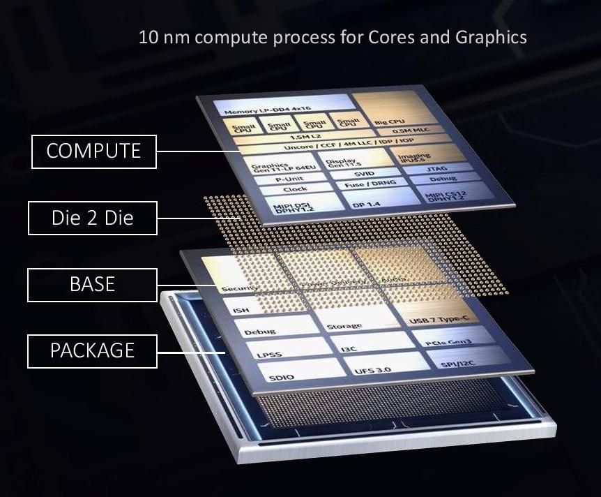
Intel’s die-to-die stacking is to a large extent very similar to the interposer technology mentioned in the EMIB section. We have one piece of silicon (or more) on top of another. In this instance however, the interposer, or base die, has active circuitry relevant for the full operation of the main compute processors found in the top piece of silicon. While the cores and graphics were on the top die in Lakefield, built on Intel’s 10nm process node, the base die had all the PCIe lanes, USB ports, security, and everything low power related to IO, and was built on a 22FFL low power process node.

So while EMIB technology splitting the silicon to work alongside each other is known as 2D scaling, by placing the silicon on top of each other we have entered a full 3D stacking regime. This comes with some good benefits, especially at scale – data paths are a lot shorter, leading to less power loss due to shorter wires but also better latency. The die-to-die connections are still bonded connections, with the first generation at a 50 micron pitch.
But there are two key limitations here: thermals and power. To avoid problems with thermals, Intel made the base die have very little logic and used a low power process. With power, the issue is enabling the top compute die to have power for its logic – this involves large power through-silicon-vias (TSVs) from the package up through the base die into the top die, and those TSVs carrying power become an issue for localized data signaling due to interference caused by high currents. There is also a desire to scale to smaller bump pitches in future processes, allowing for higher bandwidth connections, requiring more attention to be paid by the power delivery.
The first announcement related to Foveros today is regarding a second generation product. Intel’s 2023 consumer processor, Meteor Lake, has already been described above as using an Intel 4nm compute tile, taking advantage of EUV. Intel is also stating today that it will be using its second generation Foveros technology on the platform, implementing a bump pitch of 36 micron, effectively doubling the connection density over the first generation. The other tile in Meteor Lake has not been disclosed yet (either what it has or what node it is on), however Intel is also stating that Meteor Lake will scale from 5 W to 125 W.
Foveros Omni: Third Generation Foveros
For those that have been following Intel’s packaging technologies closely, then the name ‘ODI’ might be familiar. It stands for Omni-Directional Interconnect, and it was the moniker being floated in previous Intel roadmaps regarding a packaging technology that allows for cantilevered silicon. That is now going to be marketed as Foveros Omni.
This means that the limit of the first generation Foveros which needed a top die smaller than the base die is now removed. The top die can be larger than the base die, or if there are multiple die on each of the levels, they can be connected to any number of other silicon. The goal of Foveros Omni is really to solve the power problem as discussed in the initial section on Foveros – because power carrying TSVs cause a lot of localized interference in signaling, the ideal place to put them would be on the outside of the base die. Foveros Omni is a technology that allows for the top die to overhang from the base die and copper pillars are built from the substrate up to the top die to provide power.
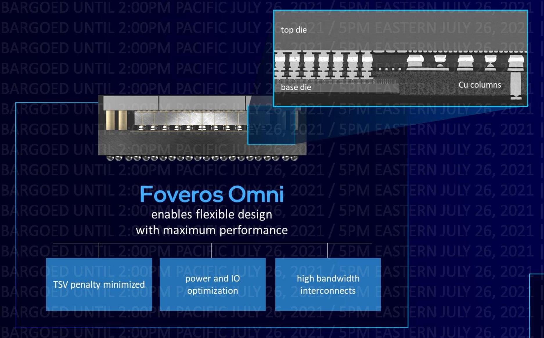
With this technology, if power can be brought in from the edges of the top die, then this method can be used. I did wonder, however, that with large silicon if power would be better fed right up the middle – Intel has stated that Foveros Omni works with split base dies, such that power carrying copper pillars could be placed in the middle of the design if the base die is designed for substrate to be available on that lower layer.
By moving the power TSVs outside the base die, this also allows for a die-to-die bump pitch improvement. Intel is citing 25 microns for Omni, which would be another 50% increase in bump density over second generation Foveros. Intel is expecting Foveros Omni to be ready for volume manufacturing in 2023.
Foveros Direct: Fourth Generation Foveros
One of the issues with any die-to-die connectivity is the connection itself. In all of these technologies mentioned so far, we’re dealing with microbump bonded connections – small copper pillars with a tin solder cap, which are put together and ‘bonded’ to create the connection. As these technologies are growing copper and the depositing tin solder, it gets difficult to scale them down, plus there is also the power loss of the electronics transferring into the different metals. Foveros Direct gets around this problem, by doing direct copper-to-copper bonding.
Rather than rely on pillars and bumps coming together, the concept of direct silicon-to-silicon connectivity has been researched for a number of years. If one piece of silicon is lined up directly with another, then there is little-to-no need for extra steps to grow copper pillars and such. The issue comes with making sure that all the connections are made, ensuring that both the top die and bottom die are so incredibly flat that nothing can get in the way. Also, the two pieces of silicon have to become one, and are permanently bonded together without any way of coming apart.
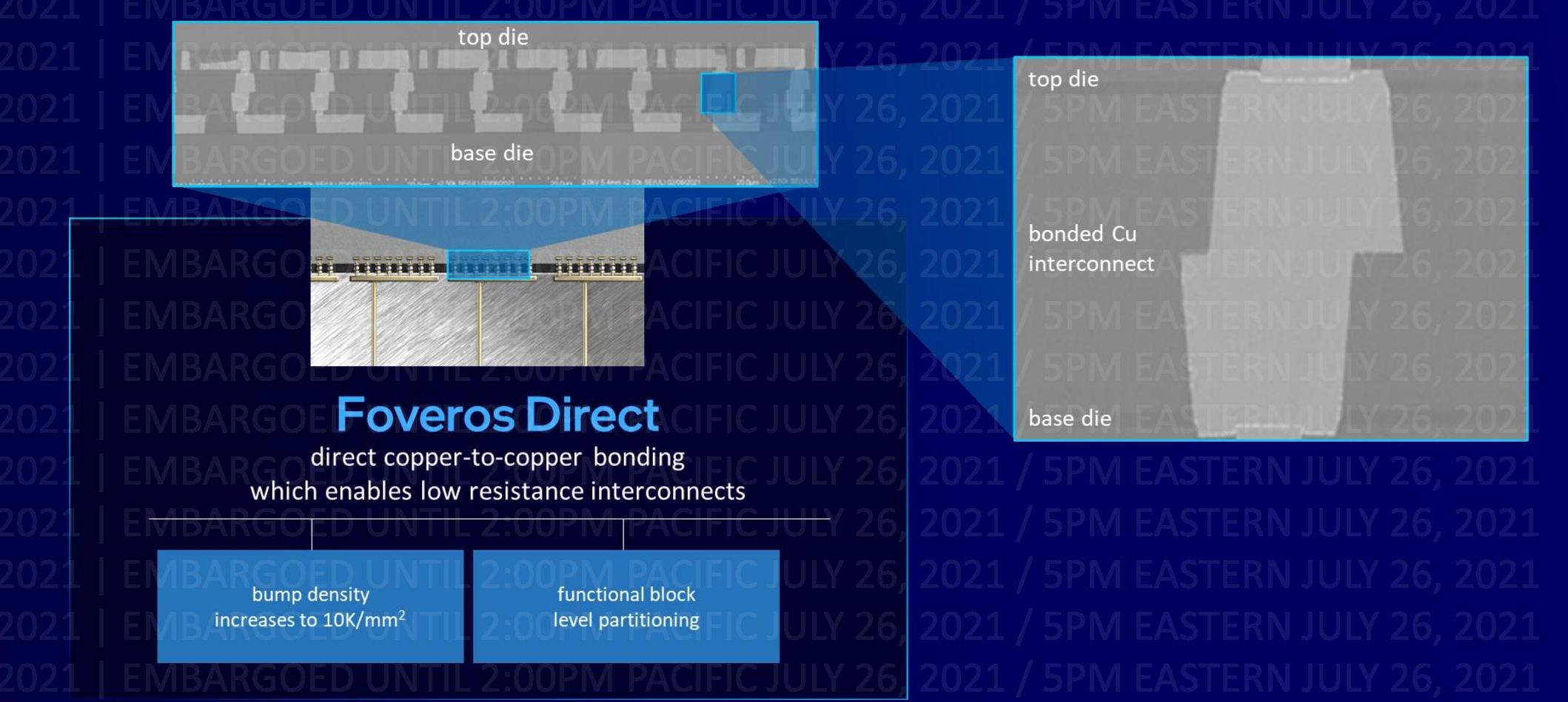
Foveros Direct is a technology that helps Intel drive the bump pitch of its die-to-die connections down to 10 micron, a 6x increase in density over Foveros Omni. By enabling flat copper-to-copper connections, bump density is increased, and the use of an all-copper connection means a low resistance connection and power consumption is reduced. Intel has suggested that with Direct, functional die partitioning also becomes easier, and functional blocks could be split across multiple levels as needed.
Technically Foveros Direct as a die-to-die bonding could be considered complimentary to Foveros Omni with the power connections outside the base die – both could be used independently of each other. Direct bonding would make internal power connections easier, but there would still be the issue of interference perhaps, which Omni would take care of.
It should be noted that TSMC has a similar technology, known as Chip-on-Wafer (or Wafer-on-Wafer), with customer products set to come to the market in the coming months using 2-high stacks. TSMC has demonstrated a 12-high stack in mid-2020, however this was a test vehicle for signaling, rather than a product. The issue going up in stacks is still going to be thermals, and what goes into each layer.
Intel predicts that Foveros Direct, like Omni, will be ready for mass volume in 2023.


326 Comments
View All Comments
JoeDuarte - Tuesday, August 3, 2021 - link
That's not how knowledge works, or how reality works. It's not possible to know the answers to these sorts of questions by a moment's reflection and opinion generation, especially when the opinions contain no real info. "smart enough to invest" is meaningless without concrete data, like how much "Taiwan" actually "invested" in TSMC, when they did so, and how this investment influenced TSMC's ability to develop new nodes, if at all.(And your second clause is probably false in that I don't think any chipmaker wastes all of their retained earnings on shareholders, and of course "wastes" is a loaded term that would have to be justified with arguments and data.)
You can't really know anything about the world around you using your method here.
mode_13h - Wednesday, August 4, 2021 - link
> You can't really know anything about the world around you using your method here.To put it another way: the term for inferencing without data is "imagination".
mode_13h - Tuesday, July 27, 2021 - link
> It would be very interesting to see some rigorous organizational research on> how some foundries are able to reliably advance with new nodes and shrinks
True. But these must be closely-held secrets. I'm sure they'd closely guard them for decades.
> it looks like Intel is simply unable to advance.
They're advancing, just slowly. They finally got 10 nm performing competitively, by the time they reached 10 nm++ (SuperFin).
And they've delivered products with Foveros and EMIB.
That's why I said above that it's not a question so much of *whether* Intel will deliver, but in what decade!
JoeDuarte - Monday, August 9, 2021 - link
Is Foveros in anything? In desktops? I haven't heard anything.I don't remember what EMIB is, but it only matters if it matters. That is, if it confers benefits to users, like speed.
I don't trust their plus sign stacking anymore, or labels like "Super"-this or that. At this point it's all going to be bottom line metrics for me re: Intel. Is it faster? How much faster? That sort of thing.
Also, it has to actually exist and be ready to buy by normal means, like Dell, Amazon, etc. If there are no desktops with SuperFin+++++ Tiger Claw, Cougar Lake, Bald Eagle Lake, Rocket Man, etc. then it's moot. I think whatever Lake is supposed to have SuperFin++++ is in desktops yet.
JoeDuarte - Monday, August 9, 2021 - link
I *don't* think...mode_13h - Tuesday, August 10, 2021 - link
> Is Foveros in anything? In desktops? I haven't heard anything.Lakefield, but I'm guessing that's why you added "in desktops". Chip development times seem to be around 4 years or so. That means you wouldn't expect an overnight transition to something like Foveros. First, it has to be proven and refined. Then, you might see chips still early in their design phase start to utilize it, but that should result in a gap between the first example and more widespread adoption. So, the fact that we haven't yet seen widespread adoption doesn't mean anything, in itself.
> I don't remember what EMIB is
It's easy to look up. It's Intel's technology for building multi-chip modules. I think Sapphire Rapids is slated to use it. Otherwise, I think Meteor Lake might be first.
> I don't trust their plus sign stacking anymore
If we were talking about 14 nm, then I'd agree. However, they've been a bit more transparent about what distinguishes 10 nm+, 10 nm++, and 10 nm+++. For details, see the article (which refers to ++ as SF and +++ as ESF).
> Is it faster? How much faster? That sort of thing.
Their foundry business should offer new transparency into their manufacturing node. Before, when Intel was practically their fabs' only customer, they didn't need to reveal detailed performance characteristics of their process iterations. However, when you're trying to attract customers to use your fabs, the standard for transparency is a lot higher. It also means that Intel needs to be more conservative about their roadmaps, since actual manufacturing contracts are going to hang by on-time and on-target delivery.
However, I agree that the end result (cost, area, power, frequency, and wafers per month) are what really matters. I'm not really bothered about dubious density metrics, and that's why I think they should just switch to a sequential version numbering scheme.
> Also, it has to actually exist and be ready to buy by normal means
Manufacturing process roadmaps are not of much interest to end-consumers, precisely because the timelines for getting end products on shelves is so far out.
Also, I'd say consumer shouldn't even think much about manufacturing tech. Good product reviews will show the relevant performance and power characteristics, and that's what most people really care about.
> I think whatever Lake is supposed to have SuperFin++++ is in desktops yet.
Ice Lake uses "regular" 10 nm, which is really 10 nm+ (but Intel doesn't call it that, because they'd rather pretend that Cannon Lake's 10 nm didn't happen). Ice Lake launched in laptops toward the end of 2019 and in servers a few months ago.
Tiger Lake uses 10 nm SF. The quad-core launched in laptops at the end of 2020 and 8-core launched a few months ago. The only "desktops" that have either are small-form-factor PCs, such as NUCs. Intel skipped selling it as a normal desktop CPU, probably due to manufacturing constraints (i.e. insufficient volume), but *maybe* also having to do with performance or power scaling.
Alder Lake should launch (for desktops!) around the end of this year and will be the first CPU on 10 nm ESF (now called "Intel 7"). It'll be the first "10 m" product they've launched for desktops.
JoeDuarte - Friday, August 13, 2021 - link
@mode_13h, Foveros isn't new though. It's old. I first read about it in 2019, or earlier. My comment rested on my unstated framing view that Foveros is old, and it's in my bucket of "Things Intel has hyped but never delivered.", like the optical Thunderbolt (Lightpeak?), Hybrid Memory Cube RAM, especially HMC2 and later, silicon photonics (as something that exists in even high-end desktops and servers), 10nm, 7nm, Phi/Knights (in computers we can buy), Panel Self-Refresh, and that optical connector embedded in functional USB ports (which would be awesome; I think Sony did something similar on a VAIO).I don't know what Lakefield is, but Googling it reveals that Intel has cancelled it, so Foveros isn't real yet, and might never be, not as something in a computer we can buy. I doubt EMIB will ever matter.
I didn't mention desktop as some sort of cynical ploy. I mentioned it because it's what I care about most, and it's also where Intel has failed to advance the most, re: 10nm etc. It's also a pet peeve of mine that desktop computing is often dismissed as unimportant because of what I call the Growth Fallacy, or the Relative Growth Fallacy. It's the fallacy that a market or industry doesn't matter, or doesn't matter much, is it's not growing at any arbitrary present. Or if some other category is growing faster, or growing a lot. Desktop is enormously important, a huge market, and where work happens. So I care most about desktop. The 7 watt stuff doesn't solve any problems for me.
mode_13h - Saturday, August 14, 2021 - link
> Foveros isn't new though. It's old.In the relative scheme of things, it's pretty new. It's also newer than the rest of the things you mentioned. And, for some of those, the issue is more that their time hasn't yet come. For instance, the OCP article (Rebecca Weekly interview) mentioned silicon photonics as an area of growing focus.
> Lakefield ... Googling it reveals that Intel has cancelled it
Not cancelled, but it reached end-of-life. There's an important difference, as one involves actually bringing a functioning product to market and supporting it.
I think Foveros is slated to appear possibly in Meteor Lake, which will be Intel's first chiplet-based desktop CPU. It's planned to come after Raptor Lake, which will follow Alder Lake. So, probably near the end of 2023. I'm not sure if they have any other products planned to use it, before then, but I wouldn't be surprised.
> desktop computing is often dismissed as unimportant
I haven't heard that, recently. For several years, the PC sector was on a slope of inexorable decline, but that changed around the time Zen launched.
> Desktop is enormously important,
It's indisputably high-profile. It was the beachfront for AMD's comeback in the CPU space, and it routinely generates lots of publicity for Nvidia and AMD's GPU products.
BTW, I'm not trying to be an Intel apologist, here. I'm just trying to present the facts as I understand them. And my understanding is that technologies like EMIB and Foveros are still in their commercial infancy. Certainty will only come with time.
AdrianBc - Tuesday, July 27, 2021 - link
To be fair, after a few years of complete stagnation, during the last 4 years Intel has improved steadily their 10 nm process.For example the maximum clock frequency has increased from 3.2 GHz in 2018 to 4 GHz in 2019, then 5 GHz in 2020 and finally 5.3 GHz (according to rumors) in 2021.
The renamed "Intel 7" manufacturing process will be the first Intel process better than the 7 nm TSMC process, if the Intel claims are true.
The problem for Intel is that this slow recovery might be too late, because meanwhile TSMC has been using already for a long time the superior 5 nm process, in high volume production (for Apple).
mode_13h - Tuesday, July 27, 2021 - link
> the maximum clock frequency has increased from 3.2 GHz in 2018 to 4 GHz in 2019,> then 5 GHz in 2020 and finally 5.3 GHz (according to rumors) in 2021.
Wow, almost like their 14 nm process!