3GAE

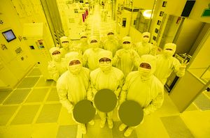
Samsung this week reported their financial results for the second quarter of 2023, closing the book on an especially bleak quarter of the year with a massive $3.4 billion operating loss. The losses, stemming from its semiconductor business, come amid a continued slump in 3D NAND and DRAM sales volumes and prices. Though buried deep in Samsung's earnings report was a speck of good news, as well: the company has started to produce its third 3nm chip design with stable yield. Discussing Samsung Foundry's earnings, the company remains uncertain about demand recovery in the second half. "Demand to recover gradually under considerable uncertainty over the intensity of a market recovery in 2H, with consumer sentiment to rebound amid easing inflation and as customers wind down...
Samsung Shipping First GAAFET Silicon; 3nm and 4nm Yields Are Improving - Report
Currently, only two foundries offer their customers 3 nm and 4 nm-class process technologies: TSMC and Samsung Foundry. But business media sometimes blames Samsung Foundry for mediocre yields on...
5 by Anton Shilov on 7/18/2023
Samsung to Unveil Refined 3nm and Performance-Enhanced 4nm Nodes at VLSI Symposium
Samsung Foundry is set to detail its second generation 3 nm-class fabrication technology as well as its performance-enhanced 4 nm-class manufacturing process at the upcoming upcoming 2023 Symposium on...
3 by Anton Shilov on 5/10/2023
Samsung Starts 3nm Production: The Gate-All-Around (GAAFET) Era Begins
Capping off a multi-year development process, Samsung’s foundry group sends word this morning that the company has officially kicked off production on its initial 3nm chip production line. Samsung’s...
22 by Ryan Smith on 6/30/2022
Applied Materials Outlines Next-Gen Tools for 3nm and GAA Transistor Era
Last month Samsung Foundry quietly announced that it was set to begin producing chips using its 3GAE (3 nm-class, gate-all-around transistors, early) process technology in the second quarter. While...
17 by Anton Shilov on 5/12/2022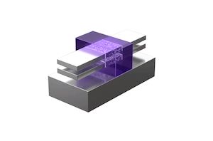
Samsung Foundry: 2nm Silicon in 2025
One of the key semiconductor technologies beyond 3D FinFET transistors are Gate-All-Around transistors, which show promise to help extend the ability to drive processors and components to higher performance...
29 by Dr. Ian Cutress on 10/6/2021
Samsung: Deployment of 3nm GAE Node on Track for 2022
Samsung Foundry has made some changes to its plans concerning its 3 nm-class process technologies that use gate-all-around (GAA) transistors, or what Samsung calls its multi-bridge channel field-effect transistors...
32 by Anton Shilov on 7/9/2021


