6nm
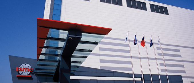
Taiwan Semiconductor Manufacturing Co. on Tuesday formally announced plans to build a second fab in Japan. The fab will be run by Japan Advanced Semiconductor Manufacturing (JASM), a majority-owned TSMC subsidiary, and will make chips on 6 nm and 7 nm-class process technologies, which will make it the most advanced semiconductor production facility for logic chips in Japan. JASM is currently gearing up to start operating its first fab in Japan. This semiconductor production facility — set to be formally opened on February 24 — will be able to process up to 55,000 300-mm wafer starts per month (WSPM) using TSMC's 40 nm, 28 nm, 22 nm, 16 nm, and 12 nm-class process technologies. This fab is set to serve needs of JASM's minor investors...

AMD Launches Zen 2-based Ryzen and Athlon 7020C Series For Chromebooks
Last year, AMD unveiled their entry-level 'Mendicino' mobile parts to the market, which combine their 2019 Zen 2 cores and their RDNA 2.0 integrated graphics to create an affordable...
33 by Gavin Bonshor on 5/23/2023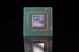
AMD Launches Mendocino APUs: Zen 2-based Ryzen and Athlon 7020 Series with RDNA 2 Graphics
Even though the main focus this month has been on AMD's upcoming launch of its Ryzen 7000 desktop series processors based on the Zen 4 architecture, AMD is also...
50 by Gavin Bonshor on 9/20/2022
TSMC and ASML: Demand for Chips Remains Strong, But Getting Fab Tools Is Hard
TSMC's revenue this year is going to set an all-time record for the company, thanks to high demand for chips as well as increased prices that its customers are...
13 by Anton Shilov on 7/21/2022
TSMC to Expand Capacity for Mature and Specialty Nodes by 50%
TSMC this afternoon has disclosed that it will expand its production capacity for mature and specialized nodes by about 50% by 2025. The plan includes building numerous new fabs...
13 by Anton Shilov on 6/16/2022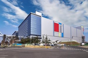
Samsung Starts Mass Production at V1: A Dedicated EUV Fab for 7nm, 6nm, 5nm, 4nm, 3nm Nodes
Samsung Foundry has started mass production of chips using its 6LPP and 7LPP manufacturing processes at its new V1 fab. The new facility employs one of the industry’s first...
30 by Anton Shilov on 2/20/2020
Samsung’s Aggressive EUV Plans: 6nm Production in H2, 5nm & 4nm On Track
Samsung Foundry formally started to produce chips using its 7LPP (7 nm low power plus) fabrication process last October and has not slowdown development of its manufacturing technologies since...
42 by Anton Shilov on 7/31/2019
TSMC: Most 7nm Clients Will Transition to 6nm
In this week's quarterly earnings conference call, TSMC’s revealed that the company expects most of its 7nm "N7" process customers to eventually transition to its forthcoming 6nm "N6" manufacturing...
39 by Anton Shilov on 5/1/2019
TSMC Reveals 6 nm Process Technology: 7 nm with Higher Transistor Density
TSMC this week unveiled its new 6 nm (CLN6FF, N6) manufacturing technology, which is set to deliver a considerably higher transistor density when compared to the company's 7 nm...
23 by Anton Shilov on 4/17/2019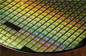
Samsung and TSMC Roadmaps: 8 and 6 nm Added, Looking at 22ULP and 12FFC
Samsung and TSMC have made several important announcements about the present and future of their semiconductor manufacturing technologies in March. Samsung revealed that it had shipped over 70 thousand...
89 by Anton Shilov on 5/5/2017


