Project Denver
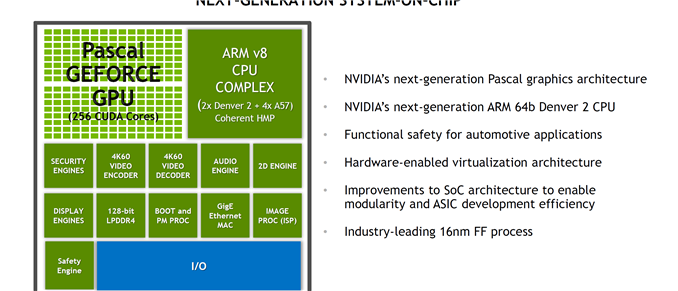
At CES 2016 we saw that DRIVE PX2 had a new Tegra SoC in it, but to some extent NVIDIA was still being fairly cagey about what was actually in this SoC or what the block diagram for any of these platforms really looked like. Fortunately, at Hot Chips 2016 we finally got to see some details around the architecture of both Tegra Parker and DRIVE PX2. Starting with Parker, this is an SoC that has been a long time coming for NVIDIA. The codename and its basic architectural composition were announced all the way back at GTC in 2013, as the successor to the Logan (Tegra K1) SoC. However Erista (Tegra X1) was later added mid-generation - and wound up being NVIDIA's 20nm generation...
The Google Nexus 9 Review
For the past few years, we’ve seen Google place significant emphasis on price as a way of competing with other tablets on the market. The original Nexus 7 managed...
169 by Joshua Ho & Ryan Smith on 2/4/2015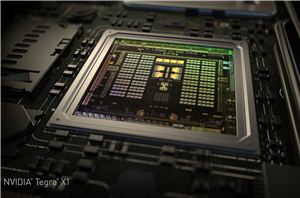
NVIDIA Tegra X1 Preview & Architecture Analysis
In the past few years, we’ve seen NVIDIA shift their mobile strategy dramatically with time. With Tegra 2 and 3, we saw multiple design wins in the smartphone space...
194 by Joshua Ho & Ryan Smith on 1/5/2015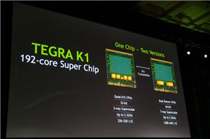
NVIDIA Reveals First Details about Project Denver CPU Core
During its CES press conference, NVIDIA revealed its new Tegra K1 SoC will be available in two versions. One version will ship with four ARM Cortex A15s, while the...
36 by Anand Lal Shimpi on 1/6/2014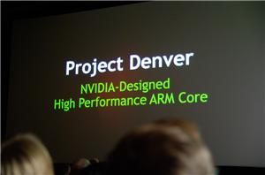
NVIDIA's Project Denver: NV Designed, High Performance ARM Core: Updated!
NVIDIA's CEO, Jen-Hsun Huang just announced Project Denver - its first CPU architecture design ever, based on ARM's ISA. This is a custom design done by NVIDIA in conjunction...
49 by Brian Klug on 1/5/2011


