TSV
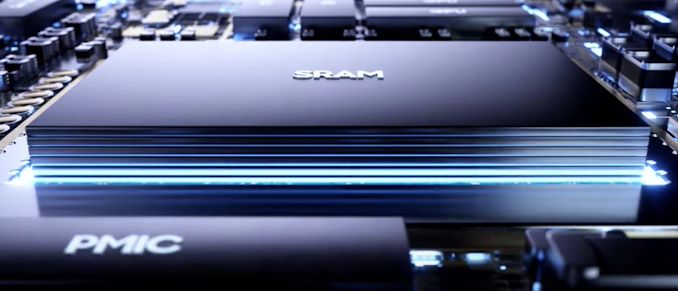
Yesterday, Samsung Electronics had announced a new 3D IC packaging technology called eXtended-Cube, or “X-Cube”, allowing chip-stacking of SRAM dies on top of a base logic die through TSVs. Current TSV deployments in the industry mostly come in the form of stacking memory dies on top of a memory controller die in high-bandwidth-memory (HBM) modules that are then integrated with more complex packaging technologies, such as silicon interposers, which we see in today’s high-end GPUs and FPGAs, or through other complex packaging such as Intel’s EMIB. Samsung’s X-Cube is quite different to these existing technologies in that it does away with intermediary interposers or silicon bridges, and directly connects a stacked chip on top of the primary logic die of a design. Samsung has built a 7nm...
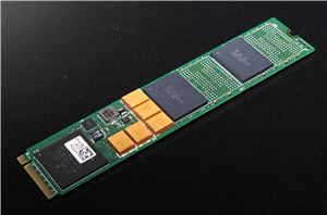
Lite-On SSDs At FMS: New Controllers And TSV NAND Packaging
Lite-On (including its consumer SSD brand Plextor) is one of the largest SSD vendors that is not vertically integrated. They don't manufacture NAND flash memory and don't design their...
1 by Billy Tallis on 8/25/2017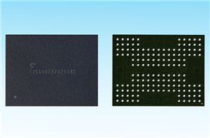
Toshiba Weds 3D NAND and TSV: Up to 1 TB 3D TLC Chips with 1066 MT/s I/O Incoming
Toshiba on Wednesday introduced its first BiCS 3D TLC NAND flash chips with 512 GB and 1 TB capacities. . The new ICs stack 8 or 16 3D NAND...
6 by Anton Shilov on 7/14/2017


