IMO this model of computing is the way the industry needs to go (pushing bits around from storage/memory to compute is wasteful of power).
HOWEVER, i also believe the adoption of this technology will be held back by the current mechanical/thermal assumptions around DRAM DIMMS which also drive electricals (spacing DIMMs out will create need for higher drive strength from the full rank of them to CPU). Someone will need to take a risk to adopt this on their server architecture.
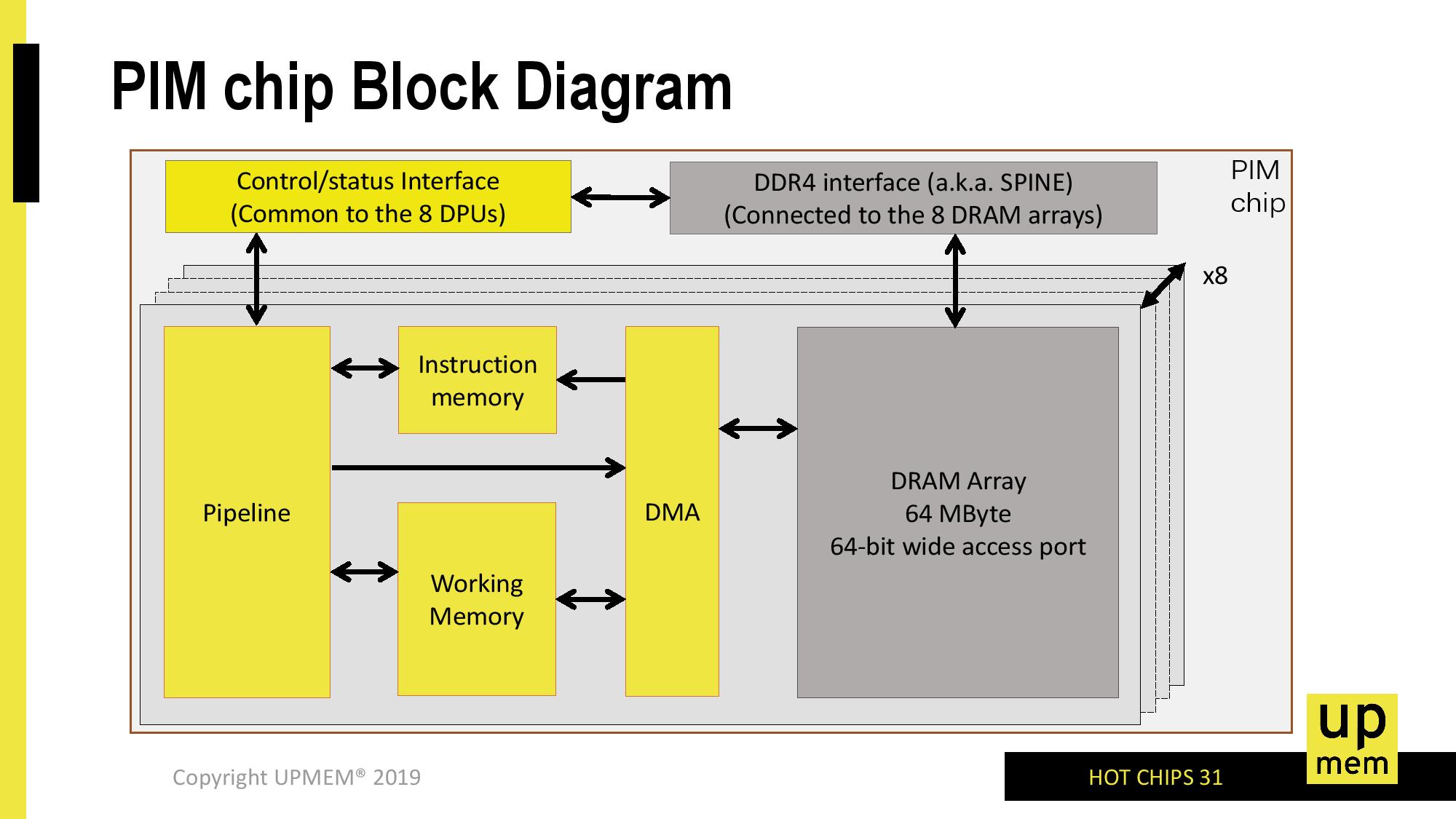
So many questions: what’s the security model? What’s the coherency model? How does virtual memory or virtualization in general interact with this? What happens when one DPU program needs data outside of its 64 MiB region?
Yeah, these two issues (security and concurrency) are the immediate sticking points, and saying that a C-library hides them doesn't help much.
An additional problem that hasn't been raised is the issue of physical address bit swizzling. Obviously this work happens at the physical address level, not virtual address; but it's worse than that. Right now physical address bits are rearranged in the memory to maximize DRAM utilization across all possible channels. So very low bits will target different memory controllers, then slightly less low bits will target ranks, and so on. Meaning that I don't understand how this "No DPU sharing" provides real value. IF DPUs can only access their own data with no DPU cross traffic, then you're limited in how much damage you can do (but you're also massively limited in how much of value you can do...) But if DPUs can write to each other (necessary if you're going to support blits and memcopy, which would seem to be the first order win) then who cares about this "no sharing", how does it help?
Onur Mutlu's solution is much less sophisticated, but also seems a lot more practical. All that solution does is perform on-DRAM blits and memcopies, in essence by allowing the CPU to send instructions through the memory controller saying copy DRAM page at address A to DRAM page at address B. This gets you most of the win, while providing no security weirdness, and a very obvious chokepoint for how you perform the virtual to (controller, rank, bank, page) mapping rather than being a nightmare for generic code.
When I invented the concept perhaps ten years ago, I called it ‘computing memory’ and I was so glad, I found no matches for it on Google. But like with many other of my ideas, plenty of others had been there and actually done something about it, too.
I was somewhat inspired by the Weitek Floating Point co-processor, an Intel i387 competitor which used a 64K memory segment while it only had perhaps 32 registers: It used the lowest significant address bit to encode one operation while writing the data, perhaps another while reading it: It very neatly solved the memory bottleneck between the CPU and the co-processor at the time, offering something like 4x the performance of Intel’s own.
Content addressable memory and the Linda Tuple space were other inspirations and I always wanted SQL-RAM, where the I’d put the WHERE clause into the address bits and then only retrieve matching data 😊.
I liked Micron's Automata Processor a lot, because it was a nice programming paradigm, good balance between problem solving power and logic overhead and excellent for formal proofs and unassailable by the likes of return oriented programming. Unfortunately they shelved that project.
HBM memory chip stacks offer free real-estate below the DRAM cells on the silicon die carrier, much like offices on the ground floor of a high-rise building with lots of elevators for the silicon tru vias (TSV). Even if the die carrier would be manufactured at a lower density, you’d have ample space for some simple logic at bandwidths much bigger than the CPU behind the chip multiplexing memory bus. I believe SK Hynix was at one point begging for engineers to come forward with ideas what to put there.
When the HP Memristor was supposed to offer 1000 layers and density at linear cost, it became very clear that general purpose CPUs simply wouldn’t be able to take advantage of that, much like a Morris Minor with 1000 BHP.
UPMEM is French I believe, I’ve heard about them for a long time, never seen a working chip yet. But computing memory is one of the few escape routes out of the von Neuman bottleneck.
Another idea was to use to expand on the row buffer also used for refresh. Use dual or tertiary buffers an a 'row ALU' that would operate on the entire memory row as a whole, e.g. for matching bit or byte patterns, then use some address bits to select transparent or operational access and write/modify the ALU row buffers.
But as I mentioned (with a bit of irony between the lines) and you noticed, I just didn't invent it first nor did I manage to put it into physical implementation.
It's rather obviously the only open avenue of escape so idea duplication is natural.
I am actually more astonished at the lack of adoption over the last years, but silicon economics is still a game of scale.
But perhaps more importantly, those companies who's rising computing-power vs. value-of- computeratio is under the strongest pressure (GAFA/BATX), have found ways to push out the energy cost onto the client devices.
It has nothing to do with adoption or scale. The materials science for modern memory technologies took a long time to catch up, some of it didn't even exist until around decade ago, and only caught up because CMOS process tech lagged and slowed down the progress of everything else.
It isn't selfish to push computing to client devices. These devices are faster to adopt optimized accelerators because they are now mostly mobile and battery restricted, which saves a tremendous amount of power overall, not just in the data-center.
We’ve updated our terms. By continuing to use the site and/or by logging into your account, you agree to the Site’s updated Terms of Use and Privacy Policy.


38 Comments
View All Comments
azazel1024 - Wednesday, August 21, 2019 - link
I prefer General In-Memory Processing. Just be careful of Last-level In-Memory Processing. I hear it can handicap your system if implemented wrong.winkingchef - Monday, August 19, 2019 - link
(This needs a #HotChips keyword tag)IMO this model of computing is the way the industry needs to go (pushing bits around from storage/memory to compute is wasteful of power).
HOWEVER, i also believe the adoption of this technology will be held back by the current mechanical/thermal assumptions around DRAM DIMMS which also drive electricals (spacing DIMMs out will create need for higher drive strength from the full rank of them to CPU). Someone will need to take a risk to adopt this on their server architecture.
Threska - Monday, August 19, 2019 - link
Basically diffusing a CPU into the space of a memory stick. Might be better to take the most used operations* in code and put those there.*Not to be confused with instructions. Too fine grained.
Elstar - Monday, August 19, 2019 - link
So many questions: what’s the security model? What’s the coherency model? How does virtual memory or virtualization in general interact with this? What happens when one DPU program needs data outside of its 64 MiB region?name99 - Saturday, August 24, 2019 - link
Yeah, these two issues (security and concurrency) are the immediate sticking points, and saying that a C-library hides them doesn't help much.An additional problem that hasn't been raised is the issue of physical address bit swizzling. Obviously this work happens at the physical address level, not virtual address; but it's worse than that. Right now physical address bits are rearranged in the memory to maximize DRAM utilization across all possible channels. So very low bits will target different memory controllers, then slightly less low bits will target ranks, and so on.
Meaning that I don't understand how this "No DPU sharing" provides real value. IF DPUs can only access their own data with no DPU cross traffic, then you're limited in how much damage you can do (but you're also massively limited in how much of value you can do...) But if DPUs can write to each other (necessary if you're going to support blits and memcopy, which would seem to be the first order win) then who cares about this "no sharing", how does it help?
Onur Mutlu's solution is much less sophisticated, but also seems a lot more practical. All that solution does is perform on-DRAM blits and memcopies, in essence by allowing the CPU to send instructions through the memory controller saying copy DRAM page at address A to DRAM page at address B. This gets you most of the win, while providing no security weirdness, and a very obvious chokepoint for how you perform the virtual to (controller, rank, bank, page) mapping rather than being a nightmare for generic code.
abufrejoval - Monday, August 19, 2019 - link
When I invented the concept perhaps ten years ago, I called it ‘computing memory’ and I was so glad, I found no matches for it on Google. But like with many other of my ideas, plenty of others had been there and actually done something about it, too.I was somewhat inspired by the Weitek Floating Point co-processor, an Intel i387 competitor which used a 64K memory segment while it only had perhaps 32 registers: It used the lowest significant address bit to encode one operation while writing the data, perhaps another while reading it: It very neatly solved the memory bottleneck between the CPU and the co-processor at the time, offering something like 4x the performance of Intel’s own.
Content addressable memory and the Linda Tuple space were other inspirations and I always wanted SQL-RAM, where the I’d put the WHERE clause into the address bits and then only retrieve matching data 😊.
I liked Micron's Automata Processor a lot, because it was a nice programming paradigm, good balance between problem solving power and logic overhead and excellent for formal proofs and unassailable by the likes of return oriented programming. Unfortunately they shelved that project.
HBM memory chip stacks offer free real-estate below the DRAM cells on the silicon die carrier, much like offices on the ground floor of a high-rise building with lots of elevators for the silicon tru vias (TSV). Even if the die carrier would be manufactured at a lower density, you’d have ample space for some simple logic at bandwidths much bigger than the CPU behind the chip multiplexing memory bus. I believe SK Hynix was at one point begging for engineers to come forward with ideas what to put there.
When the HP Memristor was supposed to offer 1000 layers and density at linear cost, it became very clear that general purpose CPUs simply wouldn’t be able to take advantage of that, much like a Morris Minor with 1000 BHP.
UPMEM is French I believe, I’ve heard about them for a long time, never seen a working chip yet. But computing memory is one of the few escape routes out of the von Neuman bottleneck.
abufrejoval - Monday, August 19, 2019 - link
Another idea was to use to expand on the row buffer also used for refresh. Use dual or tertiary buffers an a 'row ALU' that would operate on the entire memory row as a whole, e.g. for matching bit or byte patterns, then use some address bits to select transparent or operational access and write/modify the ALU row buffers.SaberKOG91 - Monday, August 19, 2019 - link
You didn't invent the idea: https://ieeexplore.ieee.org/document/592312I'm sure there are even early examples of this, but Patterson et. al were pretty prophetic in this arena.
abufrejoval - Tuesday, August 20, 2019 - link
Of course, I invented it, and all on my own, too!But as I mentioned (with a bit of irony between the lines) and you noticed, I just didn't invent it first nor did I manage to put it into physical implementation.
It's rather obviously the only open avenue of escape so idea duplication is natural.
I am actually more astonished at the lack of adoption over the last years, but silicon economics is still a game of scale.
But perhaps more importantly, those companies who's rising computing-power vs. value-of- computeratio is under the strongest pressure (GAFA/BATX), have found ways to push out the energy cost onto the client devices.
SaberKOG91 - Tuesday, August 20, 2019 - link
It has nothing to do with adoption or scale. The materials science for modern memory technologies took a long time to catch up, some of it didn't even exist until around decade ago, and only caught up because CMOS process tech lagged and slowed down the progress of everything else.It isn't selfish to push computing to client devices. These devices are faster to adopt optimized accelerators because they are now mostly mobile and battery restricted, which saves a tremendous amount of power overall, not just in the data-center.