TSMC Preps Cheaper 4nm N4C Process For 2025, Aiming For 8.5% Cost Reduction
by Anton Shilov on April 25, 2024 10:00 AM EST- Posted in
- Semiconductors
- TSMC
- 4nm
- N4
- N4C
- TSMC Symposium 2024
While the bulk of attention on TSMC is aimed at its leading-edge nodes, such as N3E and N2, loads of chips will continue to be made using more mature and proven process technologies for years to come. Which is why TSMC has continued to refine its existing nodes, including its current-generation 5nm-class offerings. To that end, at its North American Technology Symposium 2024, the company introduced a new, optimized 5nm-class node: N4C.
TSMC's N4C process belongs to the company's 5nm-class family of fab nodes and is a superset of N4P, the most advanced technology in that family. In a bid to further bring down 5nm manufacturing costs, for TSMC is implementing several changes for N4C, including rearchitecting their standard cell and SRAM cell, changing some design rules, and reducing the number of masking layers. As a result of these improvements, the company expects N4C to achieve both smaller die sizes as well as a reduction in production complexity, which in turn will bring die costs down by up to 8.5%. Furthermore, with the same wafer-level defect density rate as N4P, N4C stands to offer even higher functional yields thanks to its die area reduction.
"So, we are not done with our 5nm and 4nm [technologies]," said Kevin Zhang, Vice President of Business Development at TSMC. "From N5 to N4, we have achieved 4% density improvement optical shrink, and we continue to enhance the transistor performance. Now we bring in N4C to our 4 nm technology portfolio. N4C allows our customers to reduce their costs by remove some of the masks and to also improve on the original IP design like a standard cell and SRAM to further reduce the overall product level cost of ownership."
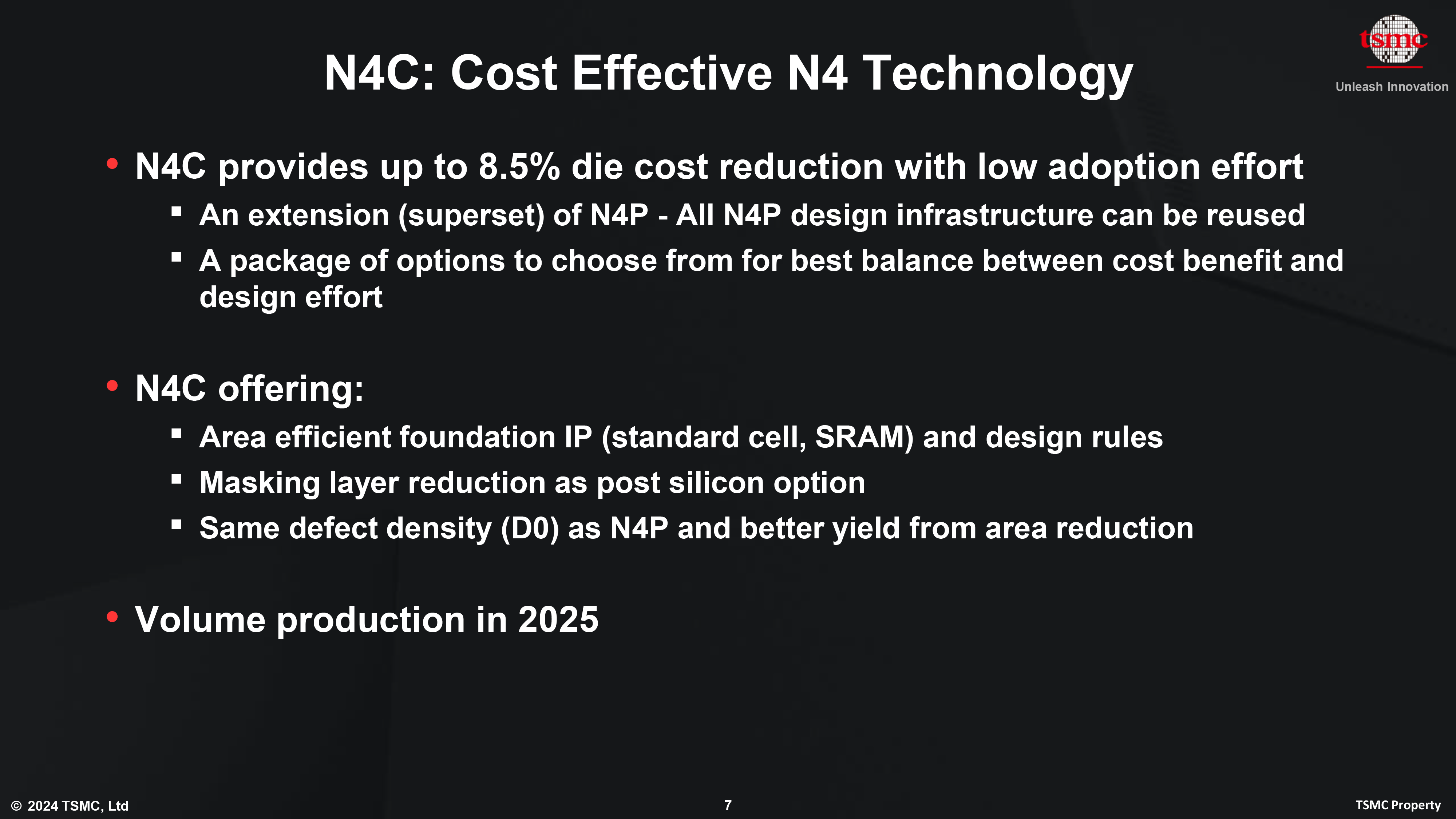
TSMC says that N4C can use the same design infrastructure as N4P, though it is unclear whether N5 and N4P IP can be re-used for N4C-based chips. Meanwhile, TSMC indicates that it offers various options for chipmakers to find the right balance between cost benefits and design effort, so companies interested in adopting a 4nm-class process technologies could well adopt N4C.
The development of N4C comes as many of TSMC's chip design customers are preparing to launch chips based on the company's final generation of FinFET process technology, the 3nm N3 series. While N3 is expected to be a successful family, the high costs of N3B have been an issue, and the generation is marked by diminishing performance and transistor density returns altogether. Consequently, N4C could well become a major, long-lived node at TSMC, serving as a good fit for customers who want to stick to a more cost-effective FinFET node.
"This is a very significant enhancement, we are working with our customer, basically to extract more value from their 4 nm investment," Zhang said.
TSMC expects to start volume production of N4C chips some time next year. And with TSMC having produced 5nm-class for nearly half a decade at that point, N4C should be able to hit the ground running in terms of volume and yields.
Related Reading
- TSMC's 1.6nm Technology Announced for Late 2026: A16 with "Super Power Rail" Backside Power
- TSMC 2nm Update: N2 In 2025, N2P Loses Backside Power, and NanoFlex Brings Optimal Cells
- TSMC's System-on-Wafer Platform Goes 3D: CoW-SoW Stacks Up the Chips
- TSMC Jumps Into Silicon Photonics, Lays Out Roadmap For 12.8 Tbps COUPE On-Package Interconnect


6 Comments
View All Comments
mczak - Thursday, April 25, 2024 - link
Unless this can be extrapolated from the text (mentioning it's a superset of N4P), there's no mention of electrical performance. So it's probably safe to asume it's no better than N4P, but hopefully not worse neither?Terry_Craig - Thursday, April 25, 2024 - link
I suspect it's a little bit better.deil - Monday, April 29, 2024 - link
Focus is elsewhere, but they would not take any major downgrades.I assume it will be single digit in any direction.
it's almost always a tradeoff, so C, most likely mean noticeably cheaper and faster production, less defect due to less complicity, but raw power draw is likely not much changed.
wrosecrans - Tuesday, April 30, 2024 - link
Guessing, but I think "C" processes are allowed to be worse performing than "P" process of the same generation, even if they come out later. In some cases, the improvements may result in better performance, but the selling point is cost. My understanding at this level is admittedly limited, but I think the cell library's main selling point being area optimization means that there's some stuff in the P process that will perform better at the cost of more area.nandnandnand - Friday, April 26, 2024 - link
Interesting in light of rumors that AMD will make some products such as "Sonoma Valley" on Samsung 4nm.Anymoore - Sunday, May 26, 2024 - link
It's implied yield is still a concern? "better yield from area reduction"