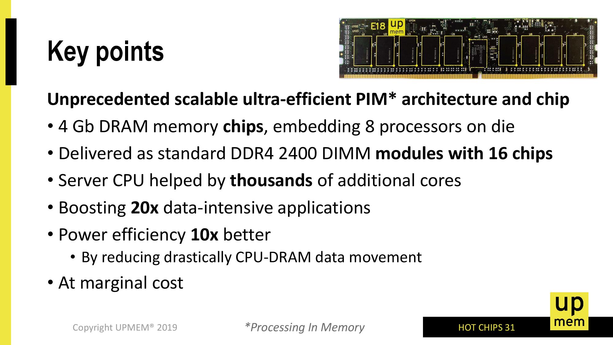
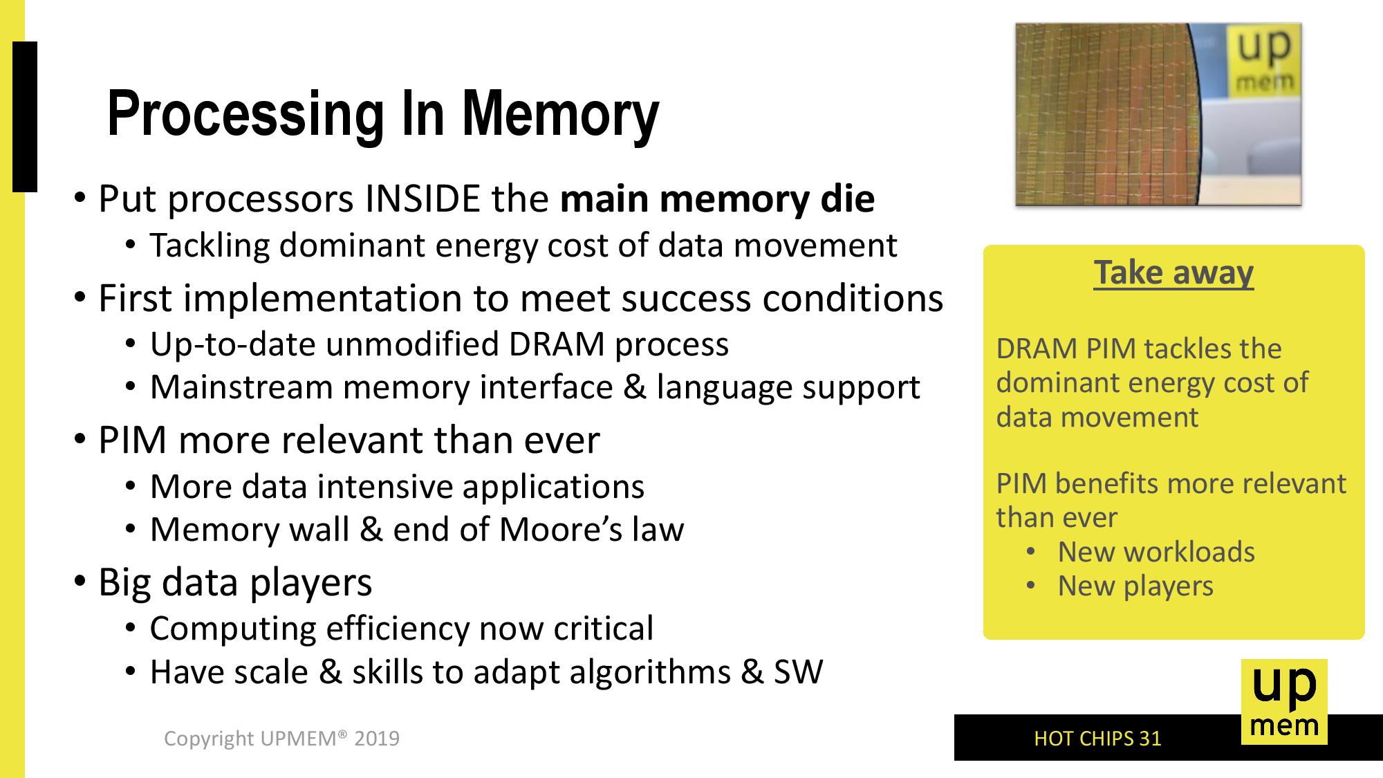
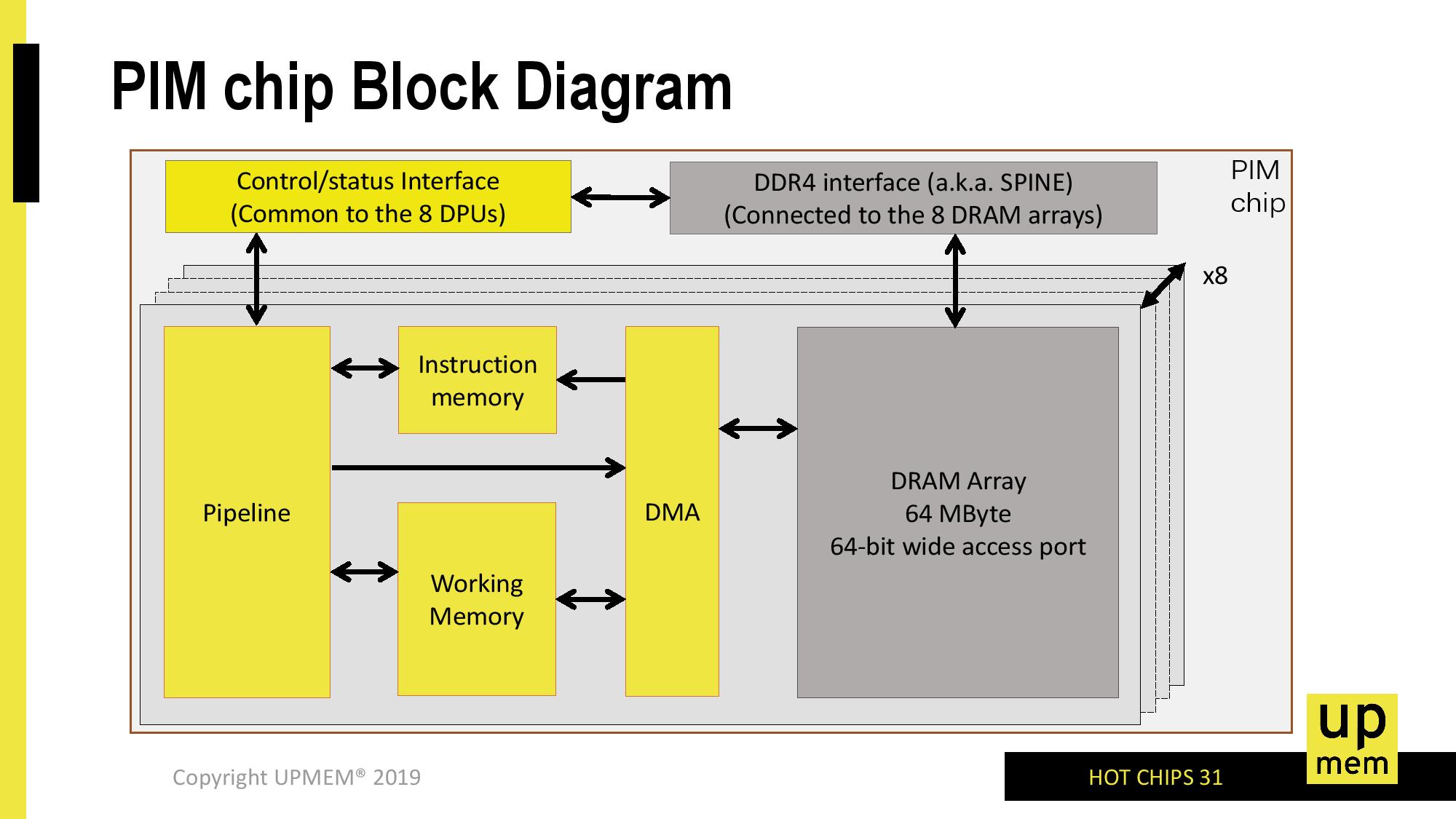
"The idea behind In-Memory Processing, or ‘Processing In-Memory’, is that a number of those simple integer or floating point operations should be done while the memory is still in DRAM – no need to cart it over to the CPU, do the operation, and then send it back."
FWIW, back in the late 70s TI built a mini, and later a chip with the ISA, which had only a couple of registers. One was an instruction pointer another was the context pointer and perhaps one or two more. All instructions were executed on memory resident data. Deja Vu all over again.
Those were stack machines and were quickly replaced by virtual machines running on RISC processors for efficiency sake. In Flynn's Taxonomy these fall more into the category of MIMD (Multiple Instruction Multiple Data) machines, whereas stack machines are SISD (Single-Instruction Single Data) machines. These chips are basically a modern take on the Stanford VIRAM processors from the late 90's early 00's. Their biggest advantage has to do with not needing to swap RAM in and out of caches to access all of it. If you could bypass the data caches and directly access RAM from the CPU you may incur higher latencies, but the energy cost wouldn't be as bad as you might think.
The TMS9900 microprocessor did indeed use a RAM based register file to save CPU transistors while supporting a full 16-bit architecture in those 8-bit days. But that was only possible because even the simplest instructions typically took several clock cycles to complete back then so the overhead of accessing a RAM based register file didn't matter that much if any: Operating on RAM didn't slow computation, truly justifying the Random Access Memory name. Today RAM is the new tape even with 3-4 levels of cache memory.
In the case of the TMS9900 data did actually get carried back and forth twice as often, as it as transferred over a multiplexed 8-bit RAM bus to the non-multiplexed 16-bit 256 Byte scratchpad RAM that represented the register file and then would do ALU operations with CPU-RAM read-write operations only to transfer the results back to ordinary RAM afterwards.
TI lost $111 on that venture, perhaps another reason not to repeat that approach.
I wonder, how memory allocation is done from point of veiw of Host? They write: work is submitted to DPU via some OS driver. Ok, this part is clear. But it is only half of the story. DPUs works with physical memory. User-level code (on host processor) works with virtual addresses. So, to prepare task for DPU it needs to know virtual to physical translation, which is typically not allowed for user programs. And even worse: it needs to allocate chunks of memory in contiguous physical (not virtual!) address space. Again, typical OSes doesn't have such API. Example: we want to add two arrays of float32 and store result into third. Let say for sake of simplicity, each source array is 16MiB. So, we need to allocate 3 chunks of 16MiB in SAME 64MiB PHYSICAL SPACE to be able to process this data with DPUs! As far as I know, no general-purpose OS supports such allocations! And it could not be solved with "simple driver", it is changes to very heart of virtual memory subsystem of OS. I can not find anything about this part in slide deck :(
That's exactly the same problem as allocating memory on GPU, though at least accessing the memory from the CPU requires only (careful - the CPU cache hierarchy doesn't know about the processors in the memory!) cache invalidation rather than trips over a PCIe bus.
One of the key critical future elements about this world of compute is moving data about. Moving data requires power, to the point where calling data from
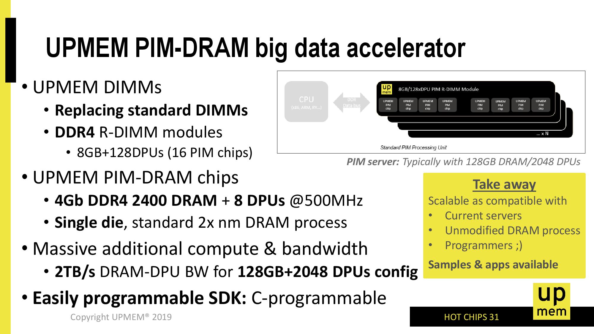
As the large bandwidth of DRAM, I guess the vector instructions will achieve more gains for upmem, but why only the scalar instructions are supported in it?
We’ve updated our terms. By continuing to use the site and/or by logging into your account, you agree to the Site’s updated Terms of Use and Privacy Policy.


38 Comments
View All Comments
philehidiot - Wednesday, August 21, 2019 - link
Kill joy. But thanks for playing along with my drunken, technically illiterate comments.FunBunny2 - Tuesday, August 20, 2019 - link
"The idea behind In-Memory Processing, or ‘Processing In-Memory’, is that a number of those simple integer or floating point operations should be done while the memory is still in DRAM – no need to cart it over to the CPU, do the operation, and then send it back."FWIW, back in the late 70s TI built a mini, and later a chip with the ISA, which had only a couple of registers. One was an instruction pointer another was the context pointer and perhaps one or two more. All instructions were executed on memory resident data. Deja Vu all over again.
SaberKOG91 - Friday, August 23, 2019 - link
Those were stack machines and were quickly replaced by virtual machines running on RISC processors for efficiency sake. In Flynn's Taxonomy these fall more into the category of MIMD (Multiple Instruction Multiple Data) machines, whereas stack machines are SISD (Single-Instruction Single Data) machines. These chips are basically a modern take on the Stanford VIRAM processors from the late 90's early 00's. Their biggest advantage has to do with not needing to swap RAM in and out of caches to access all of it. If you could bypass the data caches and directly access RAM from the CPU you may incur higher latencies, but the energy cost wouldn't be as bad as you might think.abufrejoval - Tuesday, August 27, 2019 - link
The TMS9900 microprocessor did indeed use a RAM based register file to save CPU transistors while supporting a full 16-bit architecture in those 8-bit days. But that was only possible because even the simplest instructions typically took several clock cycles to complete back then so the overhead of accessing a RAM based register file didn't matter that much if any: Operating on RAM didn't slow computation, truly justifying the Random Access Memory name. Today RAM is the new tape even with 3-4 levels of cache memory.In the case of the TMS9900 data did actually get carried back and forth twice as often, as it as transferred over a multiplexed 8-bit RAM bus to the non-multiplexed 16-bit 256 Byte scratchpad RAM that represented the register file and then would do ALU operations with CPU-RAM read-write operations only to transfer the results back to ordinary RAM afterwards.
TI lost $111 on that venture, perhaps another reason not to repeat that approach.
blacklion - Friday, August 23, 2019 - link
I wonder, how memory allocation is done from point of veiw of Host?They write: work is submitted to DPU via some OS driver. Ok, this part is clear.
But it is only half of the story. DPUs works with physical memory. User-level code (on host processor) works with virtual addresses. So, to prepare task for DPU it needs to know virtual to physical translation, which is typically not allowed for user programs.
And even worse: it needs to allocate chunks of memory in contiguous physical (not virtual!) address space. Again, typical OSes doesn't have such API.
Example: we want to add two arrays of float32 and store result into third. Let say for sake of simplicity, each source array is 16MiB. So, we need to allocate 3 chunks of 16MiB in SAME 64MiB PHYSICAL SPACE to be able to process this data with DPUs! As far as I know, no general-purpose OS supports such allocations!
And it could not be solved with "simple driver", it is changes to very heart of virtual memory subsystem of OS.
I can not find anything about this part in slide deck :(
TomWomack - Thursday, August 29, 2019 - link
That's exactly the same problem as allocating memory on GPU, though at least accessing the memory from the CPU requires only (careful - the CPU cache hierarchy doesn't know about the processors in the memory!) cache invalidation rather than trips over a PCIe bus.ThopTv - Wednesday, August 28, 2019 - link
One of the key critical future elements about this world of compute is moving data about. Moving data requires power, to the point where calling data fromSenbon-Sakura - Thursday, November 18, 2021 - link
As the large bandwidth of DRAM, I guess the vector instructions will achieve more gains for upmem, but why only the scalar instructions are supported in it?