The Apple iPhone 11, 11 Pro & 11 Pro Max Review: Performance, Battery, & Camera Elevated
by Andrei Frumusanu on October 16, 2019 8:30 AM ESTThe A13's Memory Subsystem: Faster L2, More SLC BW
The memory subsystem of a chip is an essential backbone for the performance of not only the CPU cores, but also the whole rest of the system. In this case we’re taking a closer look at how the memory subsystem behaves on the CPU side of things.
Last year we saw Apple make significant changes to the SoC’s memory subsystem with the inclusion of a new architecture system level cache (SLC), which serves as the last level cache for not only the CPU, but also a lot of other SoC components like the GPU.
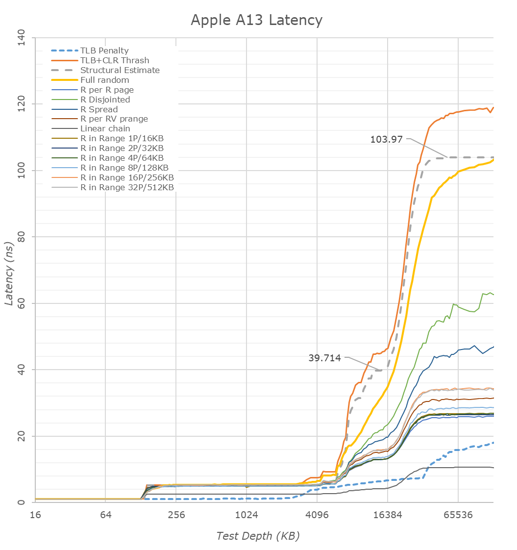
Looking first at the linear graphed memory latencies, we see that the A13’s structural DRAM latency falls in at ~104ns, a very slight regression to the 102.8ns of the A12. Apple in this regard isn’t the best among mobile SoCs, HiSilicon’s newest Kirin 990 now falls in at ~96ns and the Exynos 9820 should also fall into a similar range, however this doesn’t matter too much in the grand scheme of things given Apple’s massive cache hierarchy. Patterns such as full random pointer chasing is significantly more performant on Apple’s cores and this should be tightly linked to the strong TLBs as well as iOS’s system configuration choice of using 16KB pages.
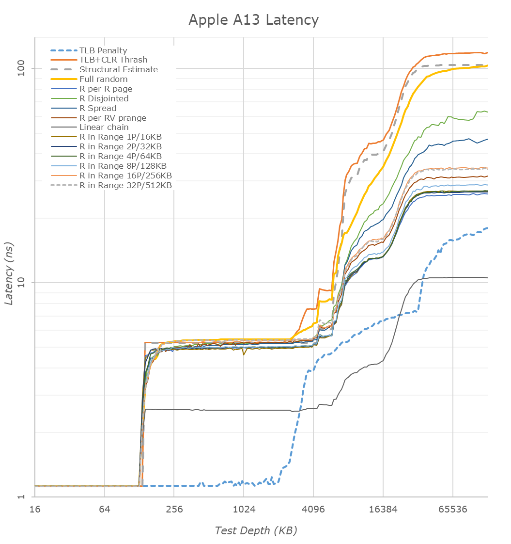
Moving to a logarithmic chart we better see the transitions between the cache hierarchies. We can clearly see Apple’s 128KB L1D cache here. The L2 cache is also relatively straightforward till 4MB as the latencies are relatively flat. From here on things become quite complicated and things differ a bit compared to the A12. Last year we determined that the L2 cache structure physically must be around 8MB in size, however we saw that it only looks as if the big cores only have access to around 6MB. Apple employs an “L2E” cache – this is seemingly a region of the big core L2 cache that serves as an L3 to the smaller efficiency cores (which themselves have their own shared L2 underneath in their CPU group).
In this region the new A13 behaves slightly different as there’s an additional “step” in the latency ladder till about 6MB. Frankly I don’t have any proper explanation as to what the microarchitecture is doing here till the 8MB mark. It does look however that the physical structure has remained at 8MB.
Going further out into the cache hierarchy we’re hitting the SLC, which would act as an L3 to the large performance cores, but should be shared with other IP blocks in the SoC. Here we see a significant change in behavior to the A12. If one had to guess as to what happening you’d think that the SLC has grown in size beyond the 8MB we estimated to have been used in the A12. Short of analyzing the die shot and see if the structure indeed has doubled, I’m a bit skeptical and I feel it’s more likely that Apple is using a partitioning system and has possibly enabled the CPU complex to access more of the SLC. What is evident here, is the doubling of the SLC cache from 8MB to 16MB.
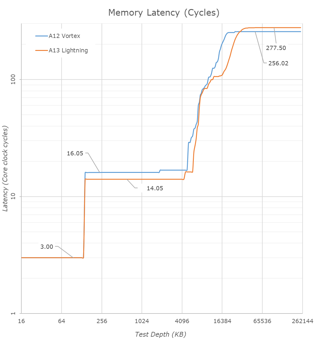
We mentioned that the Lightning cores L2 is faster now: Converting the measured latencies from nanoseconds to core cycles, we see the structural speed changes to the caches. The L1 remains at 3 cycles which is massively impressive given its 128KB size. The L2 cache has been reduced from 16 cycles down to 14 cycles, which is again extremely impressive given its purported 8MB physical size. Accounting for the core’s frequency increase, we do more noticeably see that the structural memory latency has increased a bit on the A13, adding about 21-22 cycles. It’s possible that the microarchitectural changes that made the SLC so much faster this generation had a knock-on effect in adding more total latency to DRAM.

Looking at the new Thunder cores versus last year’s Tempest microarchitecture, we see the new cache hierarchy differences. The L1D has grown from 32KB to 48KB – straightforward until now.
The L2 cache size also has evidently increased. Last year we estimated that the small core cluster had 2MB of shared L2, but was partitioned in such as way that a given core only has access to about 1.5MB, and this depth depended on the power management policy and DVFS state of the cores, appearing to only have access to 512KB when at the lowest performance states.
This year, this 1.5MB access size has seemingly increased to 2.5MB. I thus estimate the shared L2 of the small cores has increased from a physical 2MB to 3MB. Past this we’re seeing a step-wise behavior in latency up to 4MB – it’s possible this would be part of the L2E cache of the CPU complex, so in other words we’d possibly be accessing a special partition of the big core’s L2.
Update October 27th: The die shot reveals that the L2 of the Thunder cluster is half the size of the Lightning cluster L2, thus we estimate it's 4MB large in total.
In this graph we continue to see the behavior change of the A13’s SLC. At first glance it appears bigger, which still can be the case, but I rather think the CPU complex has much better access to the 4 (or more) cache slices of the SLC in this generation.
Another change of the new Thunder cores here is that we’re obviously seeing an increase in the L2 TLB capacity of the core. While the L1 TLB seems to have remained unchanged at 128 pages / 2MB, the L2 TLB has increased from 512 pages to 1024 pages – covering up to 16MB, a quite ideal size as it’s covering the depth of the SLC.
Finally, we see that the efficiency cores in the A13 this time around don’t have access to faster DRAM on their own – the memory controller remains very slow and DRAM latencies are in excess of 340ns while on the A12 the Tempest cores were able to enjoy latencies of 140-150ns. This explains some of the performance regressions of the new Thunder cores we measured earlier.
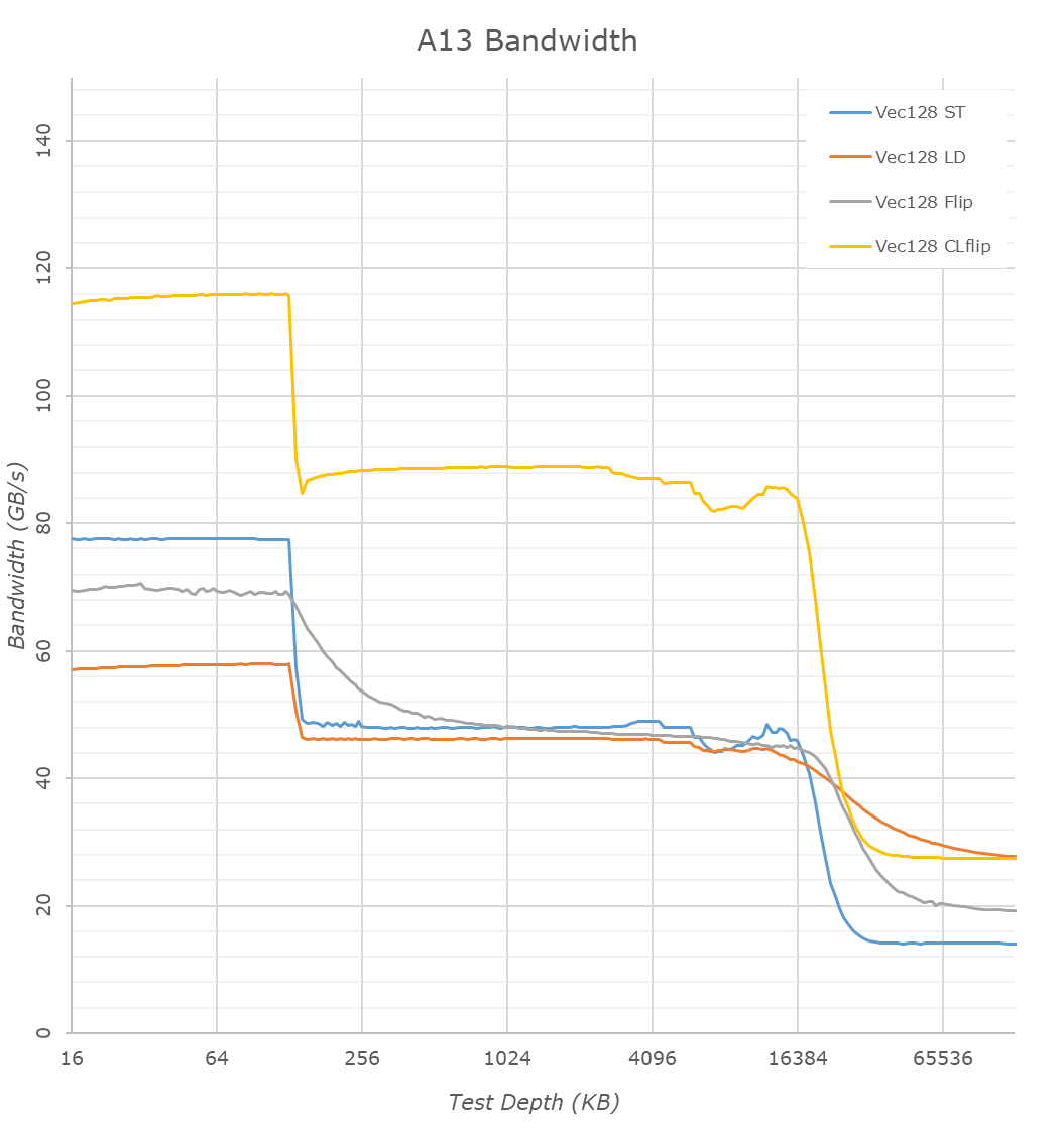
Bandwidth between the A13 and A12 doesn’t majorly differ in the L1 and DRAM regions beyond minor clock speed changes. In the L2, we notice there’s been a more noticeable increase in performance for read+writes into the same cache line, increasing performance by 25%.
It’s again in the SLC region where we see major changes – while on the A12 the bandwidth here slowly fell off in depth, the A13 is able to sustain the same bandwidth over the 16MB of system cache. It’s impressive that the bandwidth here is essentially equal to the L2 – albeit of course quite notably worse latency as we noted earlier. The smaller dips at the 8MB region is an artifact of the cache behavior between the big L2 and the SLC.
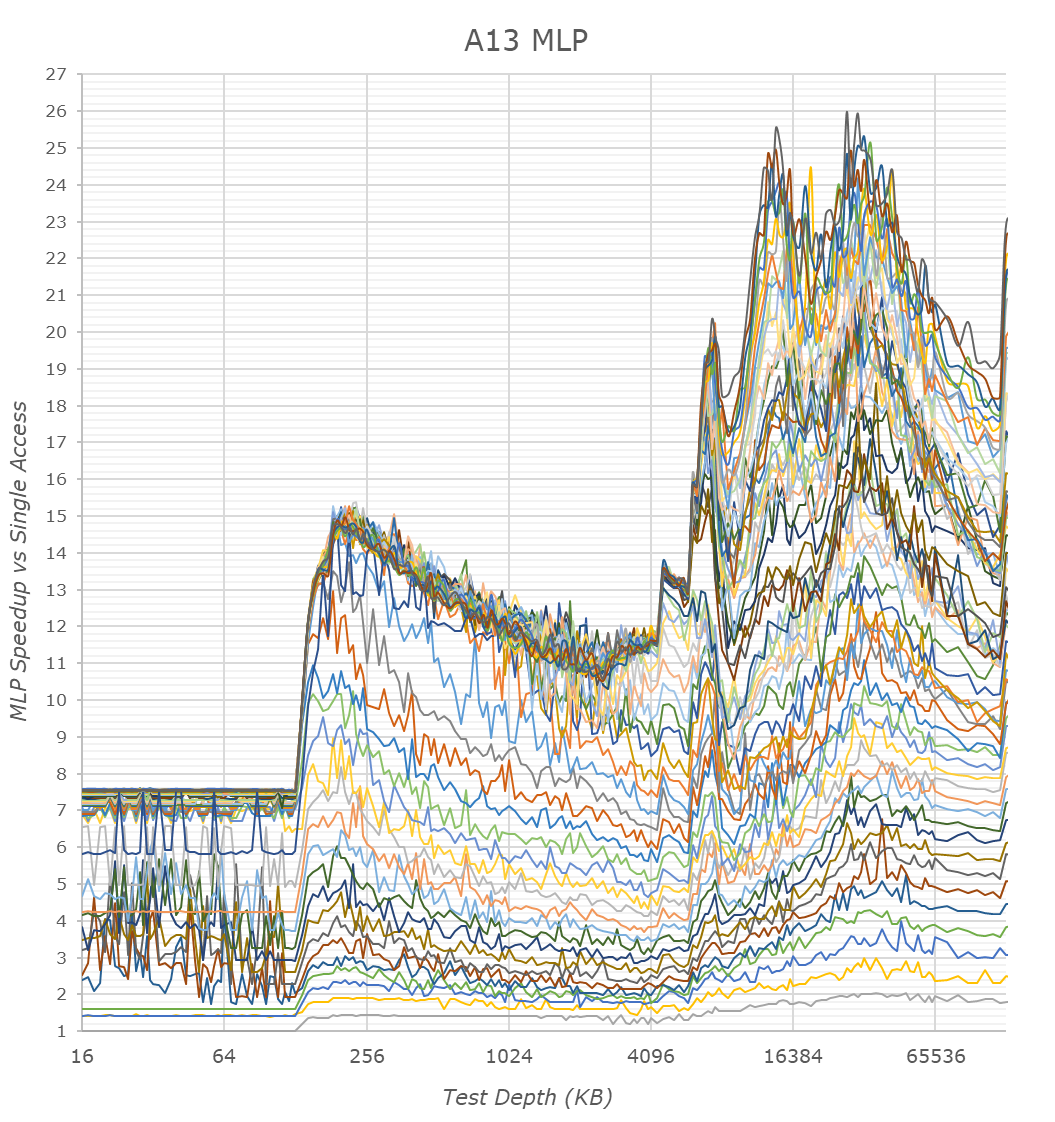
Finally, the MLP graphs showcase the memory level parallelism capacity of the CPU cores and the memory subsystem. MLP is the ability for the CPU to “park” memory requests missing the caches and to continue executing in out-of-order fashion other requests. High MLP ability is extremely important to be able to extract the most from out-of-order execution of code, which has higher memory pressure and more complex memory access patterns.
The A13 here again remains quite unique in its behavior, which is vastly more complex that what we see in any other microarchitecture. The non-linearity of the MLP speedup versus access count is something I can’t find a viable explanation for. We do see that the new A13 is a little bit better and more “even” than the A12, although what this practically means is something only Apple’s architects know. In general, Apple’s MLP ability is only second to AMD’s Zen processors, and clearly trounces anything else in the mobile space.
The overall conclusion for the A13’s memory subsystem is that Apple has evidently made very large changes to the system level cache, which is now significantly faster than what we’ve seen in the A12. The L2 cache of the big cores benefit from a 2-cycle latency reduction, but otherwise remain the same. Finally, the new Thunder efficiency cores have seen large changes with increased L1D, L2 and TLB capacity increases.


242 Comments
View All Comments
Irish910 - Friday, October 18, 2019 - link
Why so salty? If you hate Apple so much why are you here reading this article? Sounds like you’re insecure with your android phone which basically gets mopped up with by the new iPhones in every area where it counts. Shoo shoo now.shompa - Thursday, October 17, 2019 - link
Desktop performance. Do you understand the difference between CPU performance and App performance? X86 has never had the fastest CPUs. They had windows and was good enough / cheaper than RISC stuff. The reason why for example Adobe is "faster" in X86 is that Intel adds more and more specific instructions AVX/AVX512 to halt competition. Adobe/MSFT are lazy companies and don't recompile stuff for other architectures.For example when DVD encoding was invented in 2001 by Pioneer/Apple DVD-R. I bought a 10K PC with the fastest CPU there was. Graphics, SCSI disks and so on. Doing a MPEG 2 encoding took 15 hours. My first mac was a 667mhz PowerBook. The same encoding took 90 minutes. No. G4 was not 10 times faster, it was ALTIVEC that intel introduced as AVX when Apple switched to Intel. X86 dont even have real 64bit and therefore the 32bit parts in the CPU cant be removed. X86 is the only computer system where 64bit code runs slower than 32bit (about 3%). All other real 64bit systems gained 30-50% in speed. And its not about memory like PC clickers belive. Intel/ARM and others had 38bit memory addressing. That is 64gig / with a 4gig limit per app. Still, today: how many apps use more than 4gig memory? RISC went 64bit in 1990. Sun went 64bit / with 64bit OS in 1997. Apple went 64bit in 2002. Windows went 64bit after Playstation4/XboxOne started to release 64bit games.
By controlling the OS and hardware companies can optimize OS and software. That is why Apple/Google and MSFT are starting to use own SoCs. And its better for customers. There are no reason a better X86 chip cost 400 dollars + motherboard tax 100 dollars. Intel 4 core CPUs 14nm cost less than 6 dollars to produce. The problem is customers: they are prepared to pay more for IntelInside and its based on the wrong notion "its faster". The faster MSFT moves to ARM / RISCV. The better. And if the rumors are right, Samsung is moving to RISCV. That would shake up the mobile market.
Quantumz0d - Thursday, October 17, 2019 - link
Samsung just killed Texas team funding. And you don't want to pay for a socketed board and industry standard but rather have a surfacw which runs on an off the shelf processor and has small workload target in a PC ?Also dude from where you are pulling this $6 of Intel CPUs and I presume you already know how the R&D works right in Lithography ? ROI pays off once the momentum has began. So you are frustrated of 4C8T Intel monopoly amd want some magical unicorn out of thin air which is as fast that and is cheap and is portable a.k.a Soldered. Intel stagnated because of no competition. Now AMD came with better pricing and more bang for buck.
Next from Bigroom Mainframes to pocket PC (unfortunate with iOS its not because of no Filesystem anf Google following same path of Scoped Storage) microsoft put computers in homes and now they recently started moving away into SaaS and DaaS bs. And now with thin client dream of yours Itll be detrimental to the Computer HW owners or who want to own.
We do not want a Propreitary own walled gardens with orwellian drama like iOS. We need more Linux and more powerful and robust OS like Windows which handles customization despite getting sandbagged by M$ on removing control panel slowly and migrating away from Win32. Nobody wants that.
https://www.computerworld.com/article/3444606/with...
jv007 - Wednesday, October 16, 2019 - link
The lighting big cores are not very impressive this time.From 4 Watt to 5 Watt a 25% increase in power for 17% more performance.
Good for benchmarks (and the phone was actively cooled here), but not good for throttling.
7nm and no EUV, maybe next year with 5nm and EUV will improve seriously.
I wonder if we will see a A13X.
name99 - Wednesday, October 16, 2019 - link
"The lighting big cores are not very impressive this time"A PHONE core that matches the best Intel has to offer is "not impressive"?
OK then...
Total Meltdowner - Thursday, October 17, 2019 - link
Comparing this CPU to intel is silly. They run completely different instructions.Quantumz0d - Sunday, October 20, 2019 - link
It has been overblown. The Spec score is all the A series chips have. They can't replace x86 chips even Apple uses x86 cores with Linux RHEL or Free OS Linux distribution to run their services. Whole world runs on the same ISA. These people just whiteknight it like a breakthrough while the whole iOS lacks basic Filesystem access and the latest Catalina cannot run non notarized apps.Also to note the Apple First party premium optimization, that Apple pays for companies like Adobe. If you run MacOS / Trashbook Pro BGA / iOS on any non optimized SW it will be held back both on power consumption and all. It's just a glorified Nix OS and with the first party support it keeps floating. They missed out on the mass scale deployment like Windows or Linux and that's going to be their Achilles heel along with the more transformation of MacOS into iOS rather than opposite.
It's really funny when you look how 60% of the performance is max that one can get from MacOS based HW/Intel machines due to severe thinning on chassis for that sweet BGA appeal and non user serviceable HW while claiming all recycled parts and all. I'm glad that Apple can't escape Physics. VRM throttling, low quality BGA engineering with cTDP garbage etc. Also people just blatantly forget how the DRAM of those x86 processors scales with more than 4000MHz of DDR4 and the PCIe lanes it pushes out with massive I/O while the anemic trash on Apple Macs is a USB C with Dongle world, ARM replicating the same esp the Wide A series with all the Uncore and PCIe I/O support ? Nope. It's not going to happen. Apple needs to invest Billions again and they are very conservative when it comes to this massive scale.
Finally to note, ARM cannot replace x86. Period. The HPC/ DC market of the Chipzilla Intel and AMD, they won't allow for this BS, Also the ISA of x86 is so mature plus how the LGA and other sockets happen along. While ARM is stuck with BGA BS and thus they can never replace these in the Consumer market.
Let the fanboys live in their dream utopia.
tipoo - Thursday, October 17, 2019 - link
Being that the little cores are more efficient, and the battery is significantly larger, maybe they allowed a one time regresion in peak performance per watt to gain that extra performance, without a node shrink this year.zeeBomb - Wednesday, October 16, 2019 - link
the time has come.joms_us - Wednesday, October 16, 2019 - link
Show us that A13 can beat even the first gen Ryzen or Intel Skylake , run PCMark, Cinebench or any modern games otherwise this nonsense desktop level claim should go to the bin. You are using a primitive Spec app to demonstrate the IPC?I can't wait for Apple to ditch the Intel processor inside their MBP and replace with this SoC. Oh wait no, it won't happen in a decade because this cannot run a full pledge OS with real multi-tasking. =D