Intel Iris Pro 5200 Graphics Review: Core i7-4950HQ Tested
by Anand Lal Shimpi on June 1, 2013 10:01 AM EST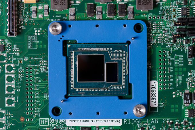
The Prelude
As Intel got into the chipset business it quickly found itself faced with an interesting problem. As the number of supported IO interfaces increased (back then we were talking about things like AGP, FSB), the size of the North Bridge die had to increase in order to accommodate all of the external facing IO. Eventually Intel ended up in a situation where IO dictated a minimum die area for the chipset, but the actual controllers driving that IO didn’t need all of that die area. Intel effectively had some free space on its North Bridge die to do whatever it wanted with. In the late 90s Micron saw this problem and contemplating throwing some L3 cache onto its North Bridges. Intel’s solution was to give graphics away for free.
The budget for Intel graphics was always whatever free space remained once all other necessary controllers in the North Bridge were accounted for. As a result, Intel’s integrated graphics was never particularly good. Intel didn’t care about graphics, it just had some free space on a necessary piece of silicon and decided to do something with it. High performance GPUs need lots of transistors, something Intel would never give its graphics architects - they only got the bare minimum. It also didn’t make sense to focus on things like driver optimizations and image quality. Investing in people and infrastructure to support something you’re giving away for free never made a lot of sense.
Intel hired some very passionate graphics engineers, who always petitioned Intel management to give them more die area to work with, but the answer always came back no. Intel was a pure blooded CPU company, and the GPU industry wasn’t interesting enough at the time. Intel’s GPU leadership needed another approach.
A few years ago they got that break. Once again, it had to do with IO demands on chipset die area. Intel’s chipsets were always built on a n-1 or n-2 process. If Intel was building a 45nm CPU, the chipset would be built on 65nm or 90nm. This waterfall effect allowed Intel to help get more mileage out of its older fabs, which made the accountants at Intel quite happy as those $2 - $3B buildings are painfully useless once obsolete. As the PC industry grew, so did shipments of Intel chipsets. Each Intel CPU sold needed at least one other Intel chip built on a previous generation node. Interface widths as well as the number of IOs required on chipsets continued to increase, driving chipset die areas up once again. This time however, the problem wasn’t as easy to deal with as giving the graphics guys more die area to work with. Looking at demand for Intel chipsets, and the increasing die area, it became clear that one of two things had to happen: Intel would either have to build more fabs on older process nodes to keep up with demand, or Intel would have to integrate parts of the chipset into the CPU.
Not wanting to invest in older fab technology, Intel management green-lit the second option: to move the Graphics and Memory Controller Hub onto the CPU die. All that would remain off-die would be a lightweight IO controller for things like SATA and USB. PCIe, the memory controller, and graphics would all move onto the CPU package, and then eventually share the same die with the CPU cores.
Pure economics and an unwillingness to invest in older fabs made the GPU a first class citizen in Intel silicon terms, but Intel management still didn’t have the motivation to dedicate more die area to the GPU. That encouragement would come externally, from Apple.
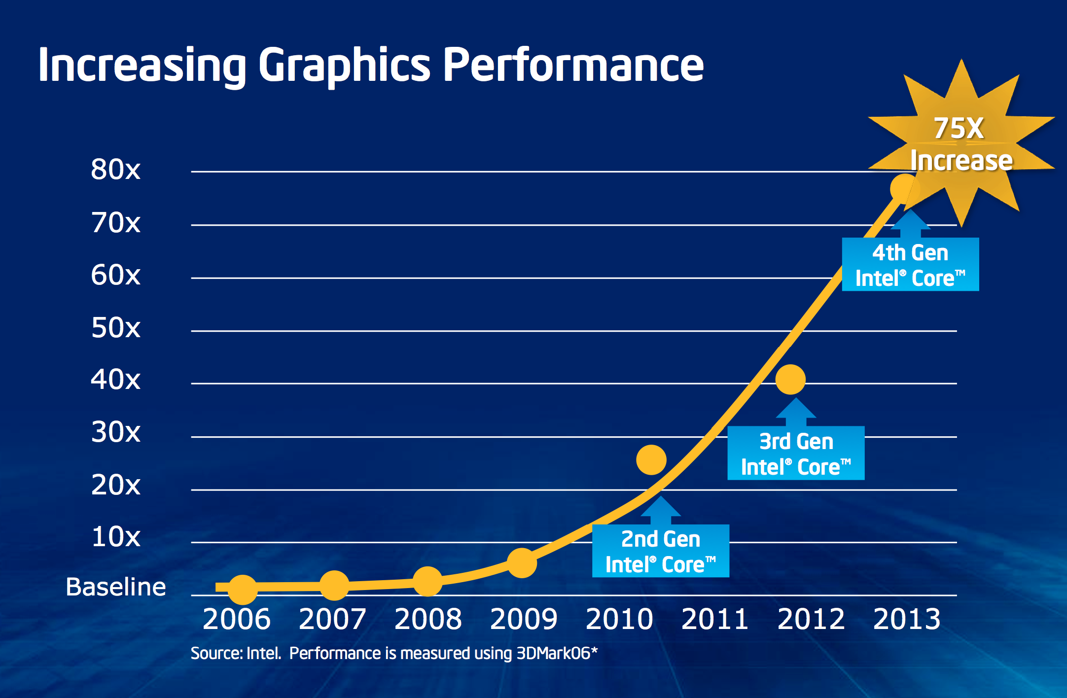
Looking at the past few years of Apple products, you’ll recognize one common thread: Apple as a company values GPU performance. As a small customer of Intel’s, Apple’s GPU desires didn’t really matter, but as Apple grew, so did its influence within Intel. With every microprocessor generation, Intel talks to its major customers and uses their input to help shape the designs. There’s no sense in building silicon that no one wants to buy, so Intel engages its customers and rolls their feedback into silicon. Apple eventually got to the point where it was buying enough high-margin Intel silicon to influence Intel’s roadmap. That’s how we got Intel’s HD 3000. And that’s how we got here.


177 Comments
View All Comments
arjunp2085 - Sunday, June 2, 2013 - link
I was under the impression that Richland has been selling on newegg as per a comment on an earlier article..I was also wondering since you had done a review on Richland from MSI notebook review i was wondering if you would do a similar comparison..
http://www.anandtech.com/show/6949/msi-gx70-3be-ri...
It would be appreciated just placing all the possible matches on the table and a paragraph with selection criteria for the review making the choices dispelling opinion of missing any models
GameHopper - Sunday, June 2, 2013 - link
Why no real power measurements? If it's so important to iris Pro, real world power numbers will be more useful than just listing TDP of the partsshinkueagle - Sunday, June 2, 2013 - link
The GIANT has awoken! Performance-wise, its amazing! Destroys Trinity! Price-wise.... Well, the area needs some work...trip1ex - Sunday, June 2, 2013 - link
Yes really disappointed there is no socketed cpu solution that have the best igpu config.But I suppose I already have Ivy Bridge i5 for my WMC pc and it is good enough. Still be a nice cheap way to build a secondary small desktop that could also do some light gaming.
Lataa - Sunday, June 2, 2013 - link
dikicha23@gmail.comvFunct - Sunday, June 2, 2013 - link
Curious why Intel just doesn't go straight for the jugular and release a discrete GPU part on their 22nm process. NVidia/AMD is stuck at 28mm because of their foundries, and it appears Intel's GPU architecture is feature complete and therefore competitive with the discrete parts if they scaled up everything by 4x or 5x.NVidia & AMD should be worried about their core high-profit-margins business!
jamescox - Sunday, June 2, 2013 - link
The photo you have on page 4 showing the 2 separate die is strange. The haswell die should not be square. Other photos I have seen show the expected (extremely rectangular) haswell die and a tiny ram chip. I would expect a haswell based chip with double the cpu (8 real cores), and no gpu eventually; this would be almost square. Do you know why your chip does not match other multi-chip module photos online?jamescox - Tuesday, June 4, 2013 - link
I guess the other photos are haswell plus an integrated chipset in the same module. The photo of the two die is still strange, as neither of these look like a haswell die.IntelUser2000 - Tuesday, June 4, 2013 - link
That's because that's the picture for GT3e Iris Pro 5200 graphics. The bigger square die is the Haswell CPU+GT3 GPU, while the smaller one is the on-package DRAM.The dual core with on-package chipset is even longer than the regular Haswell.
tipoo - Wednesday, January 21, 2015 - link
Yes it should, you're thinking of the ultrabook chips with a controller to the side, not eDRAM. Those ones are rectangular. Look at a haswell MBP 15" teardown to verify.