Hot Chips 2016: NVIDIA Pascal GP100 Die Shot Released
by Ryan Smith on August 23, 2016 12:40 AM EST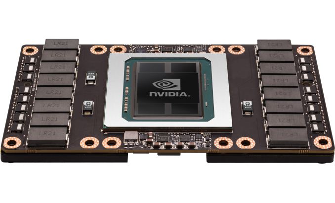
The first day of conference sessions wrapped up earlier this evening at the annual Hot Chips symposium. One of the computing industry’s lower-key events, the IEEE conference for high performance chips is not a venue for product announcements, but instead a more focused conference for tech companies and their engineers to let their hair down a bit and present some deeper technical workings of their products. Even these aren’t full product briefings – since they’re often for future products – but it’s a good venue to dive a little deeper and learn a little bit more about the technologies and decisions that have gone into putting these chips together.
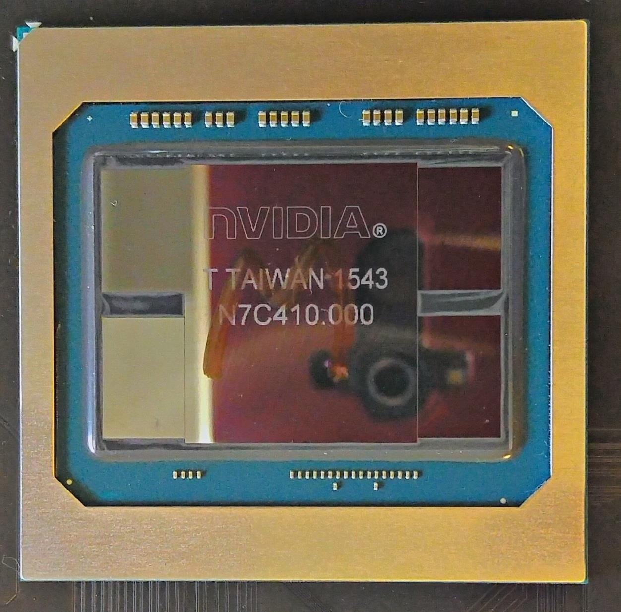
Over the next two days we’ll be covering the highlights of several presentations, but I wanted to start this year’s coverage off with some nerdy pictures. I am of course referring to die shots, as NVIDIA has released the first die shot of their behemoth 610mm2 GP100 die as part of a presentation on Pascal and NVLink 1.0. Die shots have been relatively rare in the GPU industry in recent years, particularly those for the highest-end GPUs with the most features.

GP100 is particularly interesting because it’s the first NVIDIA part featuring HBM and NVLink, two interfaces which (at least for NVIDIA) premiered on GP100. The die shot itself is not significantly enhanced (and I’m not going to spoil a good die shot here), but even with just basic coloring you can make out features such as the thread scheduler and other uncore features in the center, along of course with the SMs. GP100, as a reminder, has 60 in all, organized into 30 TPCs, the latter of which is what you’re probably counting right now.
Top and bottom of this picture appear to be the HBM2 interfaces. Despite the width of GP100’s 4096-bit HBM2 bus, the space consumed by HBM2 appears to be relatively small on the admittedly large GPU, which is one of the benefits of HBM as it allows for very tight routing and simpler GPU-side logic. Going HBM didn’t just get NVIDIA more memory bandwidth, but I fully expect it also got them a meaningful increase in die area that they could dedicate to GPU logic.
Meanwhile the presentation also gives us our best shot to date of a full (and presumably production) GP100 package. Note the tight spacing between the HBM2 stacks and the GPU die; NVIDIA did not waste any space here, as the memory stacks have been placed as close as they can be. Both the memory and GPU sit on top of the silicon interposer, itself not much larger than the hardware it sits on. Due to the large size of GP100, every millimeter ends up mattering here, as the resulting interposer has to be quite large even with this dense packing. This also does a great job illustrating just how much larger HBM2 stacks are than HBM1 stacks, as they now are a considerable fraction of the die size of GP100 itself, as opposed to the smaller HBM1 stacks used on AMD's Fury X last year.
The big question, of course, is when this technology will trickle down into cheaper, consumer-level boards. Right now HBM2 is still quite expensive, while GDDR5X has allowed NVIDIA to cover much of their bandwidth needs on consumer parts with the cheaper memory technology. However as we’ll see in the Hot Chips memory presentation, Samsung and Xilinx have some ideas on how to handle that…


13 Comments
View All Comments
Laxaa - Tuesday, August 23, 2016 - link
Will you be covering info on the new Tegra?Ryan Smith - Tuesday, August 23, 2016 - link
Yes. Josh will be working on that one. Just keep in mind that Hot Chips is a high level overview. So a deep dive would be for a review (or at least later on when we can get our hands on an actual chip).III-V - Tuesday, August 23, 2016 - link
Wow, that die shot doesn't look like something a clown puked up. Nvidia, are you feeling okay? You're acting strange.Michael Bay - Tuesday, August 23, 2016 - link
>doesn`tAre you implying a typical die shot should look like clown`s puke, or am I misreading this?
MrSpadge - Tuesday, August 23, 2016 - link
No he doesn't imply it should be this way. He implies that would be the usual way nVidia handles this.III-V - Tuesday, August 23, 2016 - link
Nvidia has a tendency to publish die shots that are either an "artist's representation" of the die and are fairly censored (e.g. Tegra, Maxwell), or have unnatural rainbow color schemes with certain areas highlighted. This one isn't exactly a "natural" die shot either, but it's much closer than what they've published since Fermi.close - Tuesday, August 23, 2016 - link
Team Green :).Freakie - Tuesday, August 23, 2016 - link
"the latter of which is what you’re probably counting right now"Rats! Foiled again!
HollyDOL - Tuesday, August 23, 2016 - link
Tbh that green die shot remotely resembles a used USD notes print matrix. Wonder if it is really green originally or postprocessed.JMC2000 - Wednesday, August 24, 2016 - link
Wow... I figured HBM2 would be somewhat larger than HBM1, but good lord, those are (relatively) massive!I wonder if SKHynix' HBM2 could come in a smaller package, if Nvidia used Samsung's.