Hot Chips 2018: Nanotubes as DRAM from Nantero, a Live Blog
by Ian Cutress on August 21, 2018 1:40 PM EST
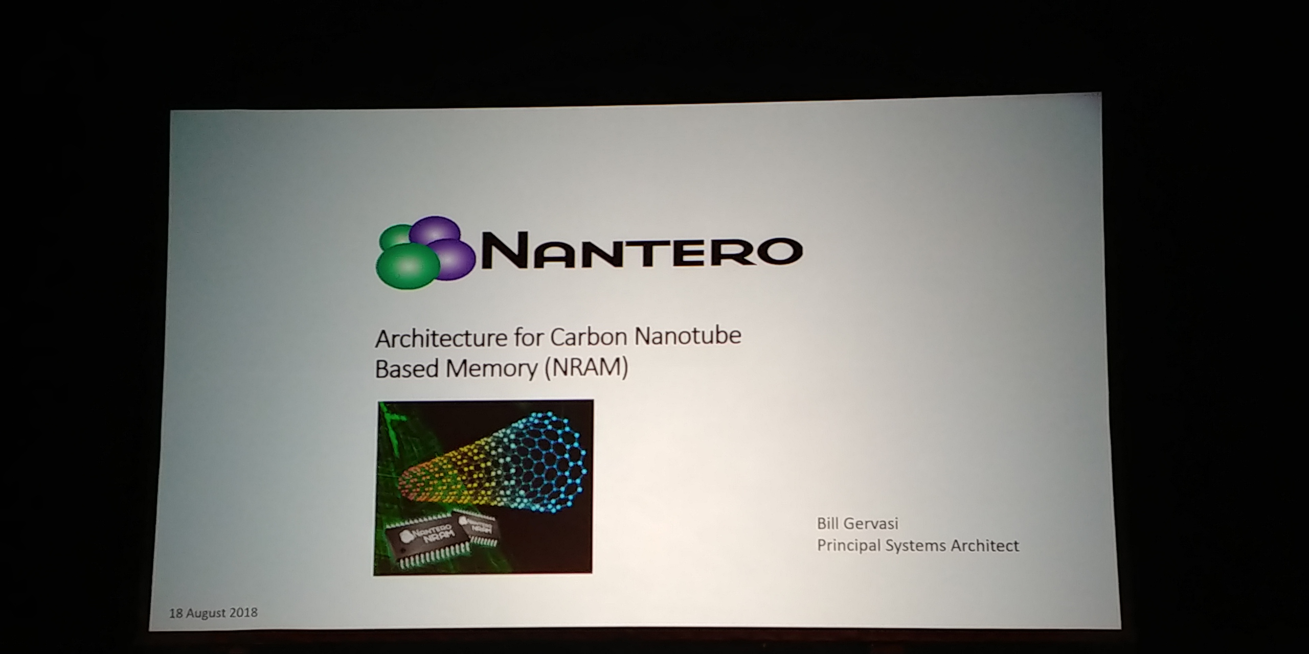
01:44PM EDT - Lots of different types of 'RAM' have been in the news, most noticably Intel's Optane memory and a couple of weeks ago at Flash Memory Summit we had the 'MRAM' Developer Day. At Hot Chips, Nantero is presentation about its new 'NRAM' technology, which uses carbon nanotubes. The talk is set to start at 10:45am PT.
01:47PM EDT - Carbon Nanotube Memory sounds sexy
01:47PM EDT - Go through Nanotubes to Memory in the talk
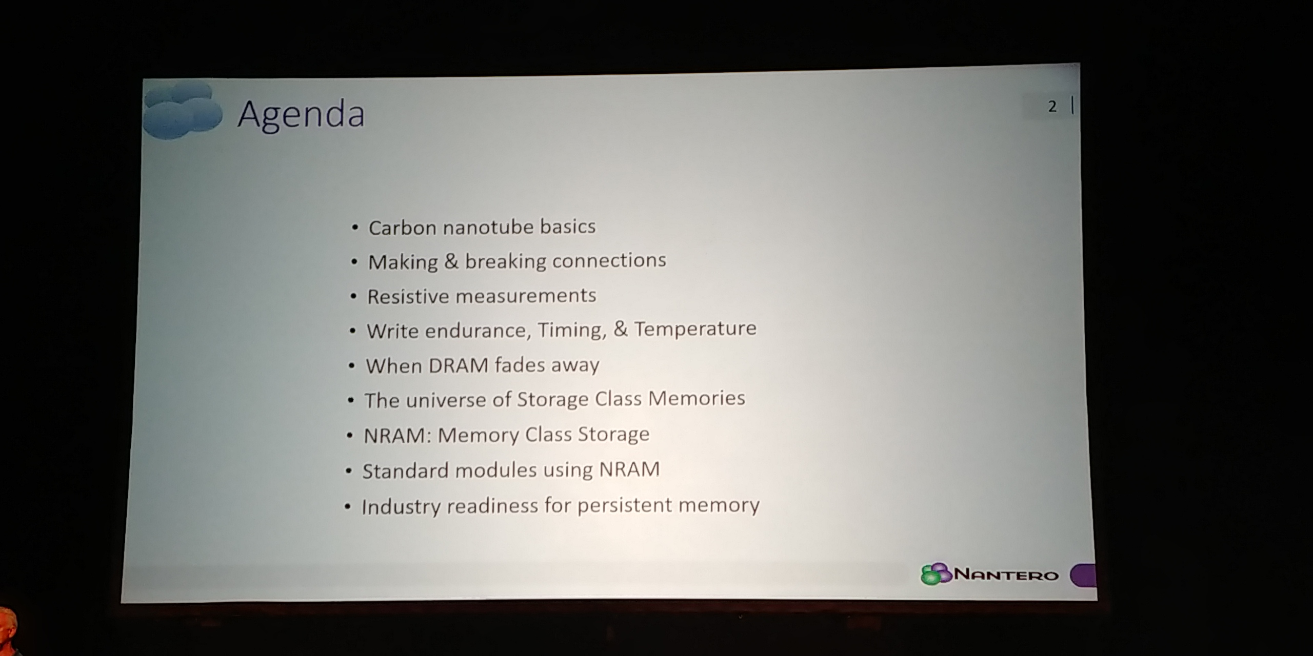
01:48PM EDT - A solution to replace DRAM
01:48PM EDT - 'Memory-class storage'
01:48PM EDT - Nantero is like Arm but for memory technology
01:49PM EDT - Specific details about marketing will depend on Nantero's customers
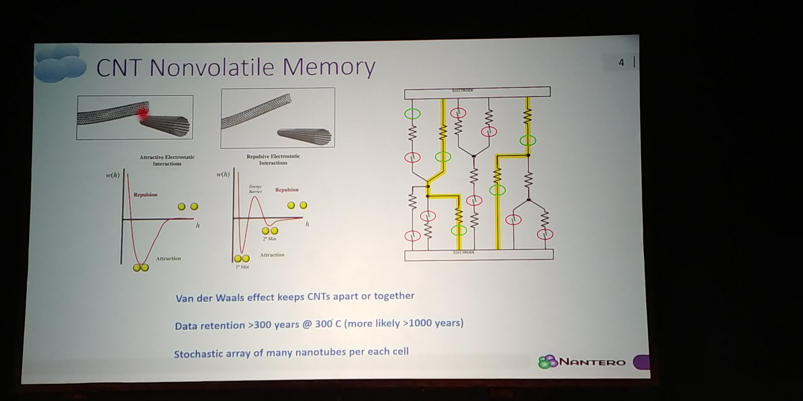
01:49PM EDT - Based on van-der-Walls effects
01:49PM EDT - Once connected, always connected
01:49PM EDT - Switched via electrostatic charges
01:50PM EDT - Use stochasic arrays of many nanotubes
01:50PM EDT - network of resistive elements
01:50PM EDT - an electrostatic force combines 1000 of cells together to lower resistance
01:50PM EDT - All the fun stuff happens at the bottom of the cell
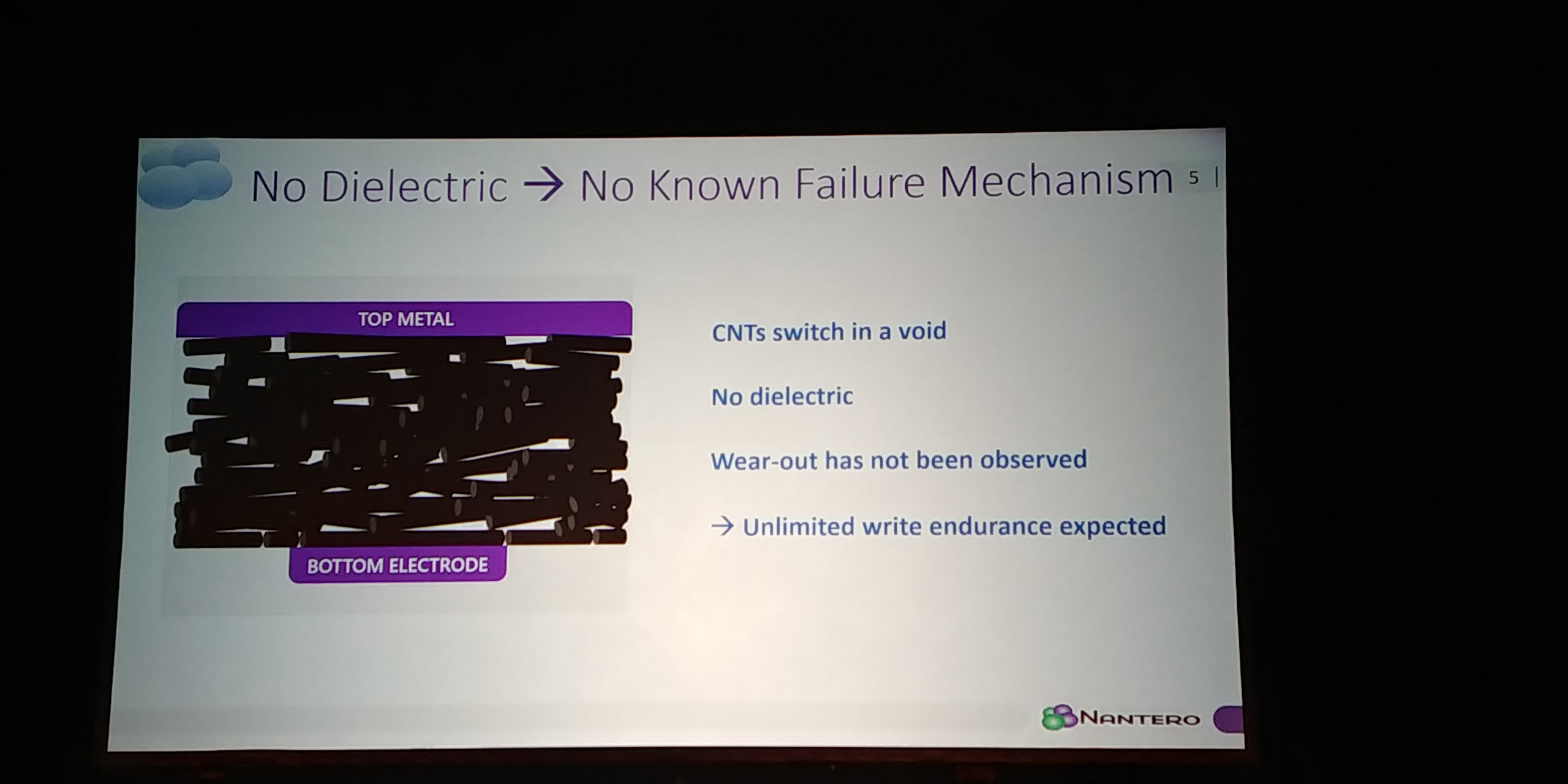
01:51PM EDT - Part of the magic is how the nanotube is selected: length and diameter
01:51PM EDT - too long will short out the switch. too short will stand up
01:51PM EDT - Don't let the carbon nanotubes at the top to move
01:51PM EDT - manufacturing process is simple
01:52PM EDT - Build the logic you need, on any process or geometry
01:52PM EDT - expose contacts, spin nanotube slurry, and bake it. Metal, etch, and seal
01:52PM EDT - 10-to-1 set to reset states in resistance
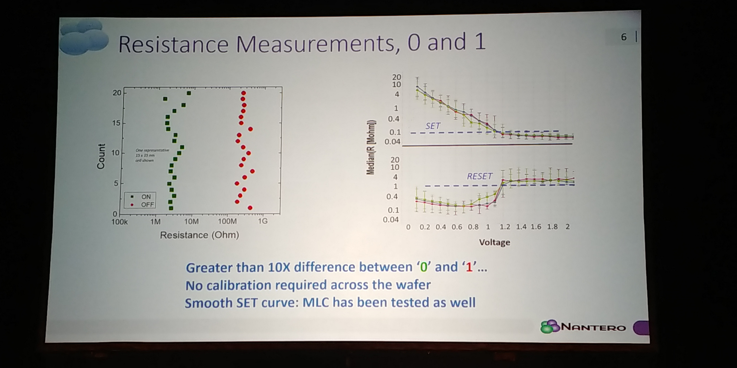
01:53PM EDT - Begun analysis of Multi-Level Cells
01:53PM EDT - Look at MLC after SLC in production
01:53PM EDT - Scales down to 15nm
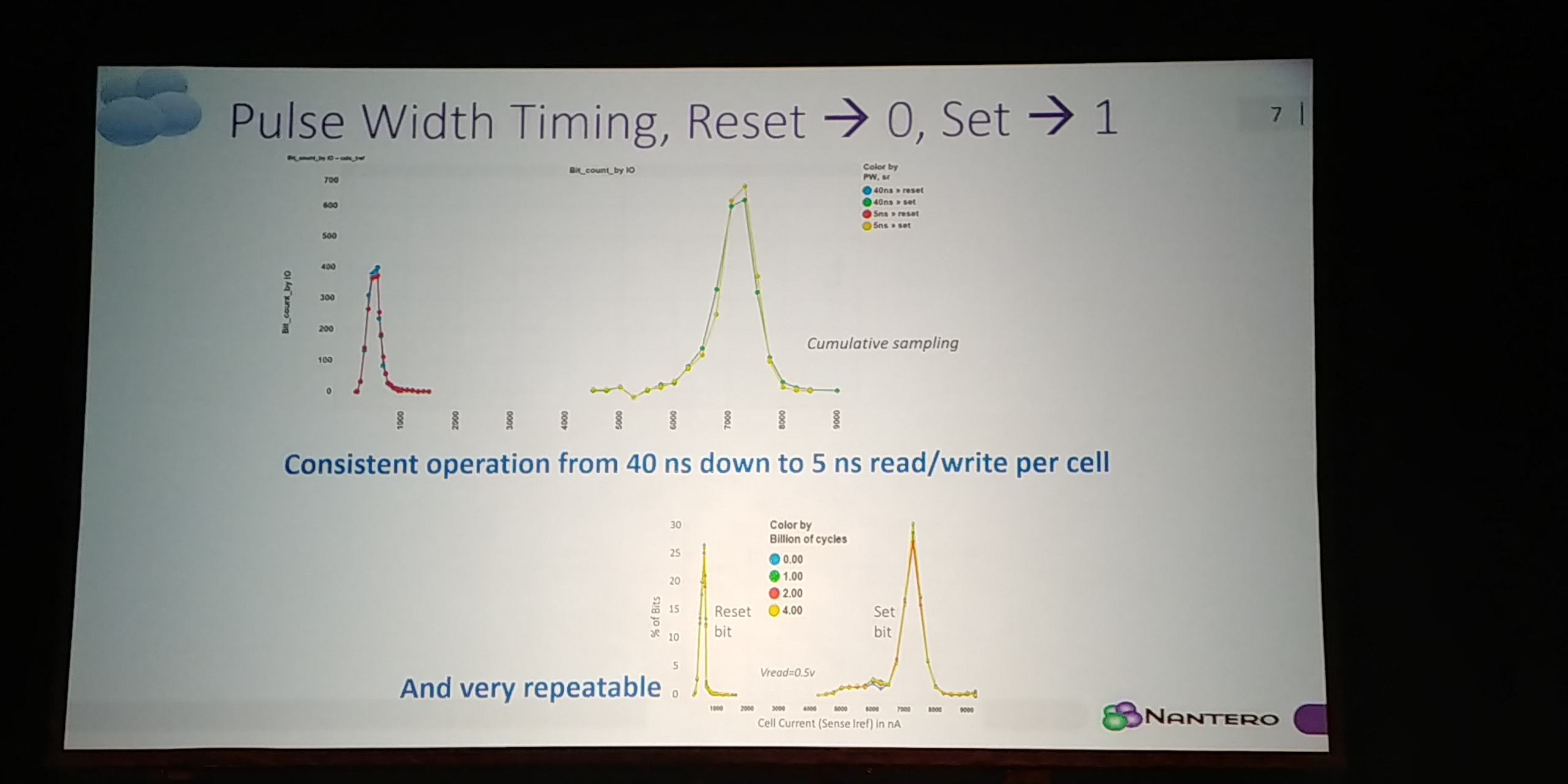
01:54PM EDT - consistent performance over billions of cycles
01:54PM EDT - Only temperature sensitivity above 300C, drops to 300 years. Otherwise 10000 years
01:54PM EDT - Believe it will scale to 5nm at a minimum
01:55PM EDT - Even at 1nm, have enough nanotubes to still change
01:55PM EDT - It's all about the length and diameter of nanotubes scaling
01:55PM EDT - Process agnostic
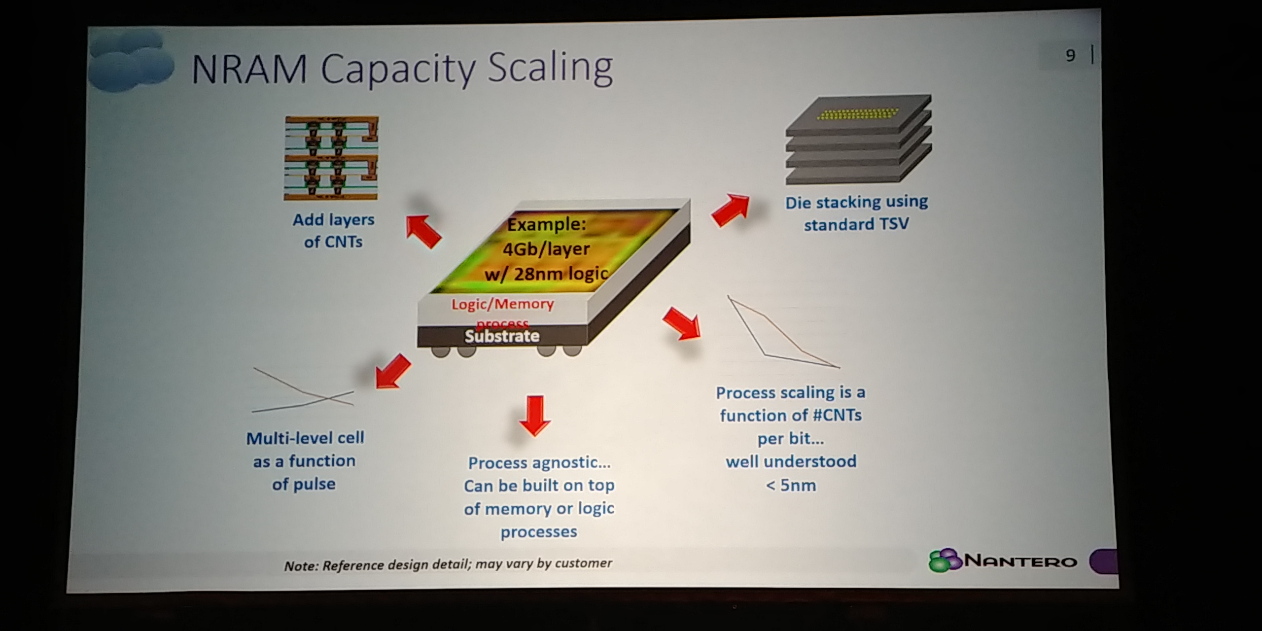
01:55PM EDT - on 28nm layer, 4Gb per layer in roughly 100mm2 die
01:55PM EDT - Also scale by adding layers
01:56PM EDT - Repeat nanotube deposit, metal, etch, deposit, metal, etch for layers
01:56PM EDT - Add layers of CNTs, or adding layers via TSVs
01:57PM EDT - Design for for DDR4 DRAM replacement device
01:57PM EDT - drop in replacement
01:57PM EDT - same timing, same perf, unlimited write endurance
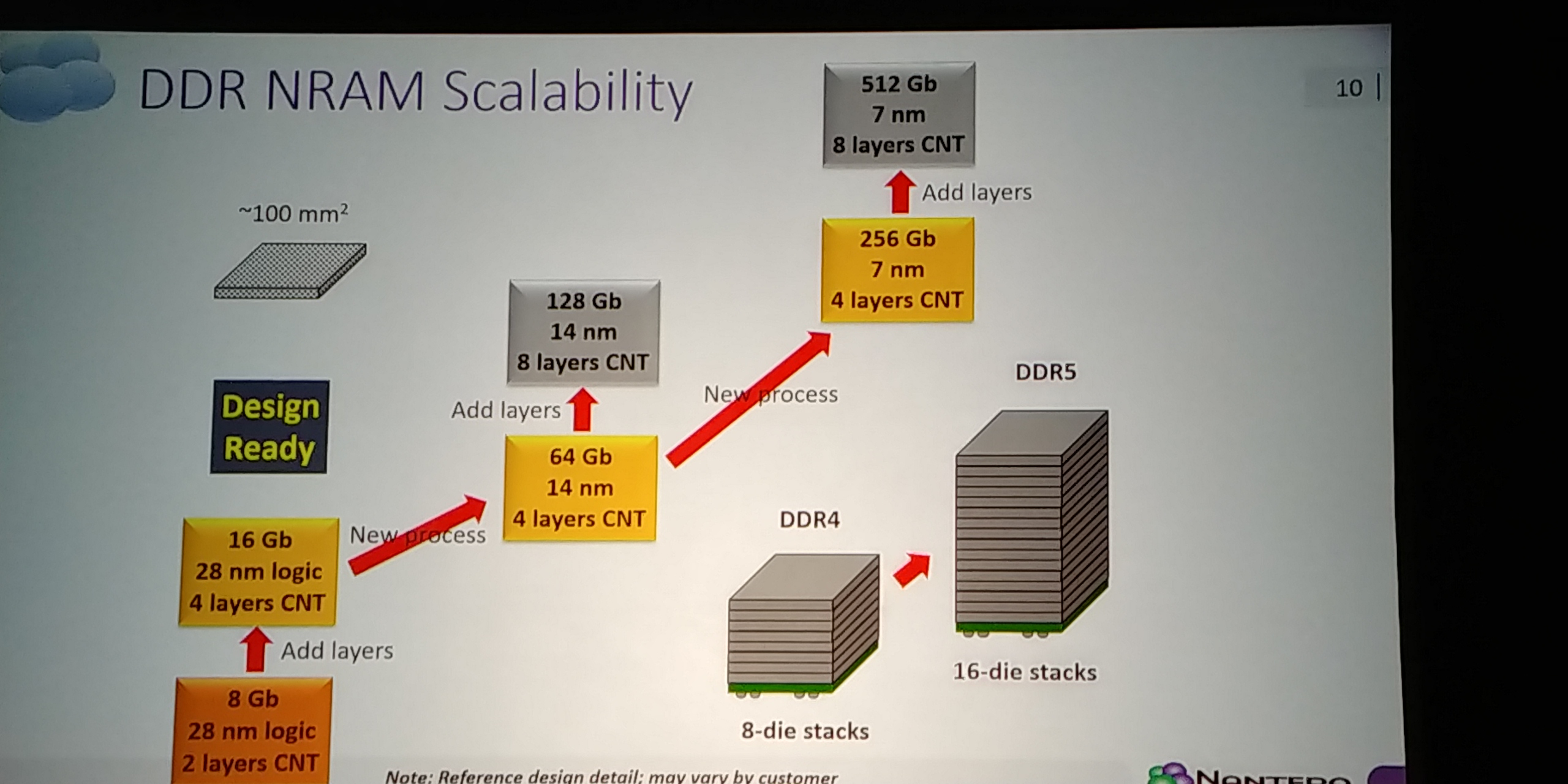
01:57PM EDT - on 28nm, get 16Gb chip with 4 layers
01:57PM EDT - in a few years, easily 14nm or 7nm for 64 Gb / 256 Gb per die
01:57PM EDT - or add layers
01:58PM EDT - DDR4 to DDR5, whcih allows for additional die stacks
01:58PM EDT - Lots of capacity in every part
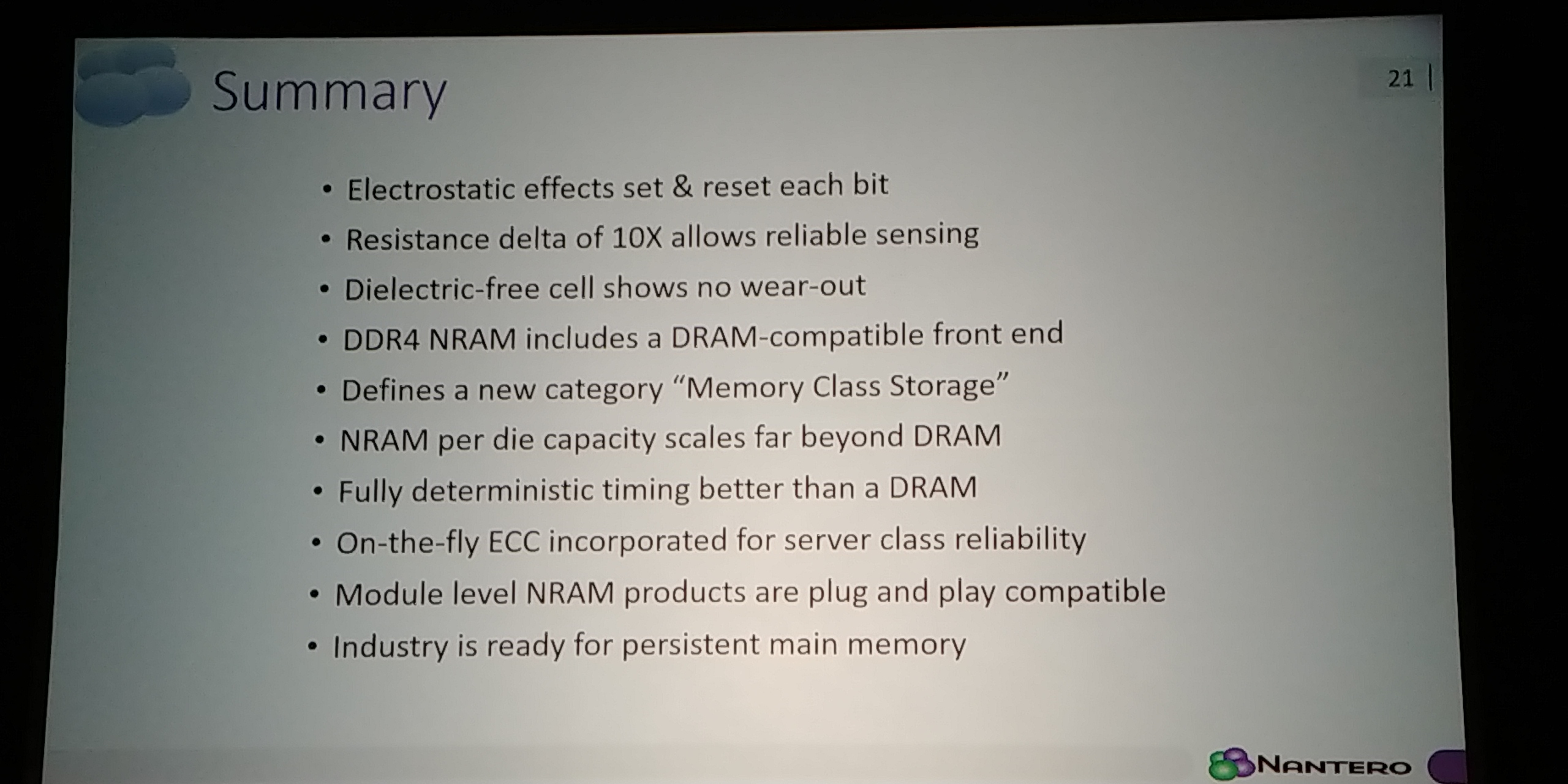
01:58PM EDT - NRAM is a storage class memroy
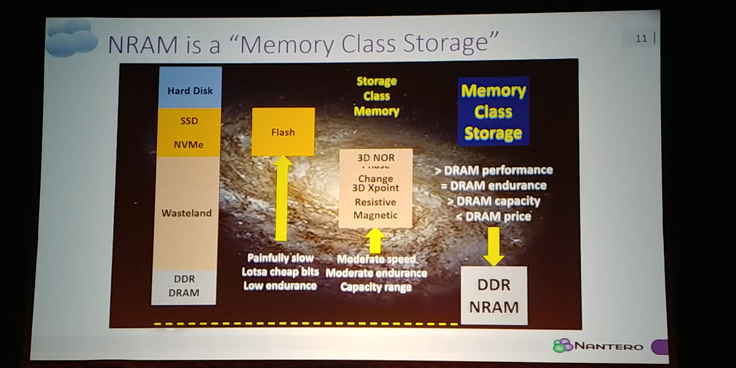
01:59PM EDT - NRAM is the only memory targeting a direct DRAM replacement

01:59PM EDT - unlimited endurance, same perf, better capacity, cheaper than DRAM
01:59PM EDT - Internal tiled architecture for memory
02:00PM EDT - Built in self-test and remapping logic for post-packaging repair
02:00PM EDT - SECDED engine in device
02:00PM EDT - in case problems with mass production - should increase yield and improve UX
02:01PM EDT - Aiming for DDR4 with ECC and to hit JEDEC standard on timings
02:01PM EDT - Decode logic in each tile with latching sense amplifiers
02:01PM EDT - Can do non-destructive read

02:01PM EDT - No things like pre-charge
02:01PM EDT - so faster :)
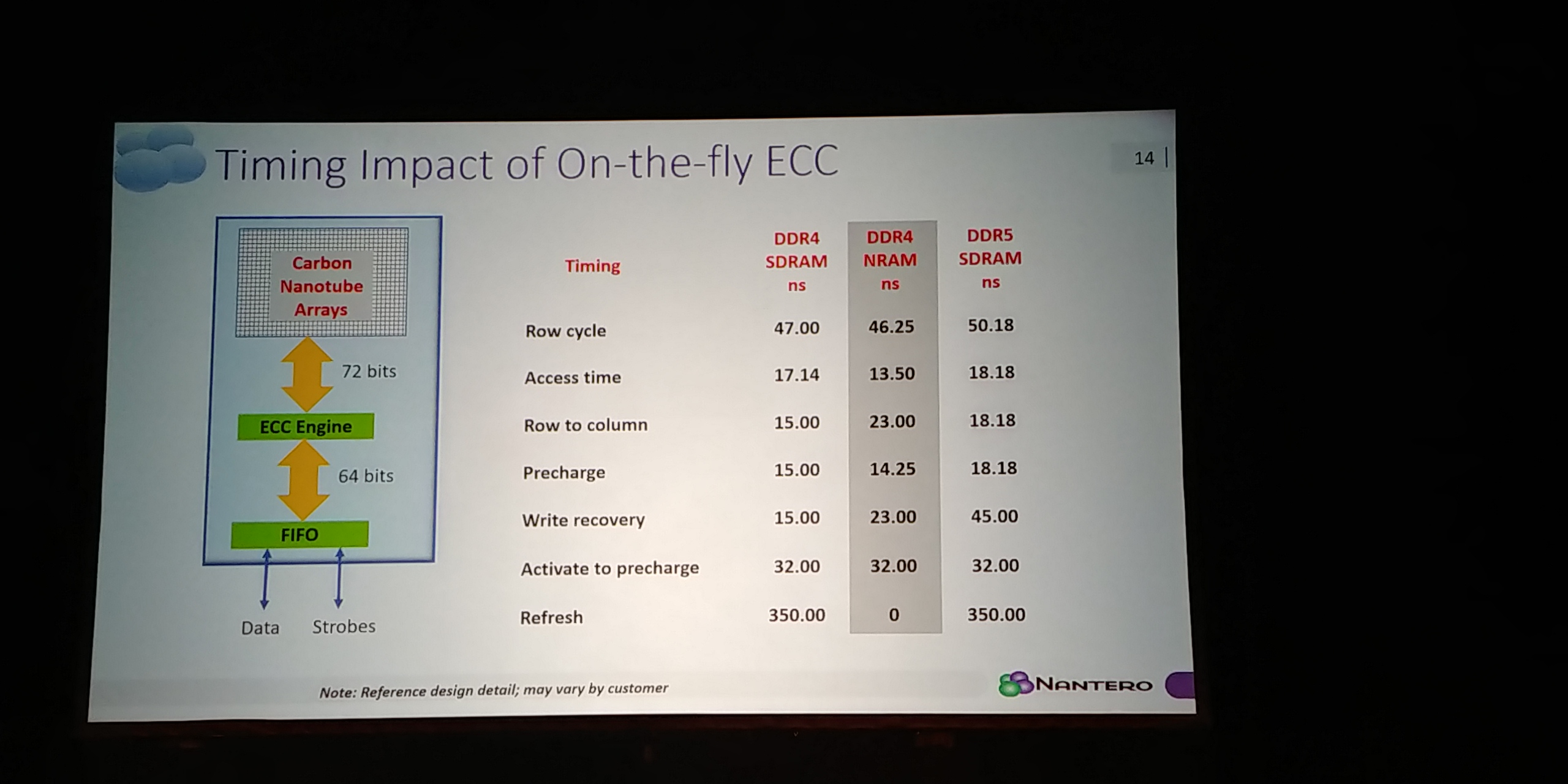
02:02PM EDT - Can now fit ECC into DDR4 timing easily due to no refresh
02:02PM EDT - 350ns to 0 ns
02:02PM EDT - DRAMs should be deterministic, but they're not due to refresh
02:02PM EDT - The DRAM should be ready when you need it
02:03PM EDT - Every 2 microseconds, need to refresh for 15% of the time
02:03PM EDT - This cuts into bandwidth
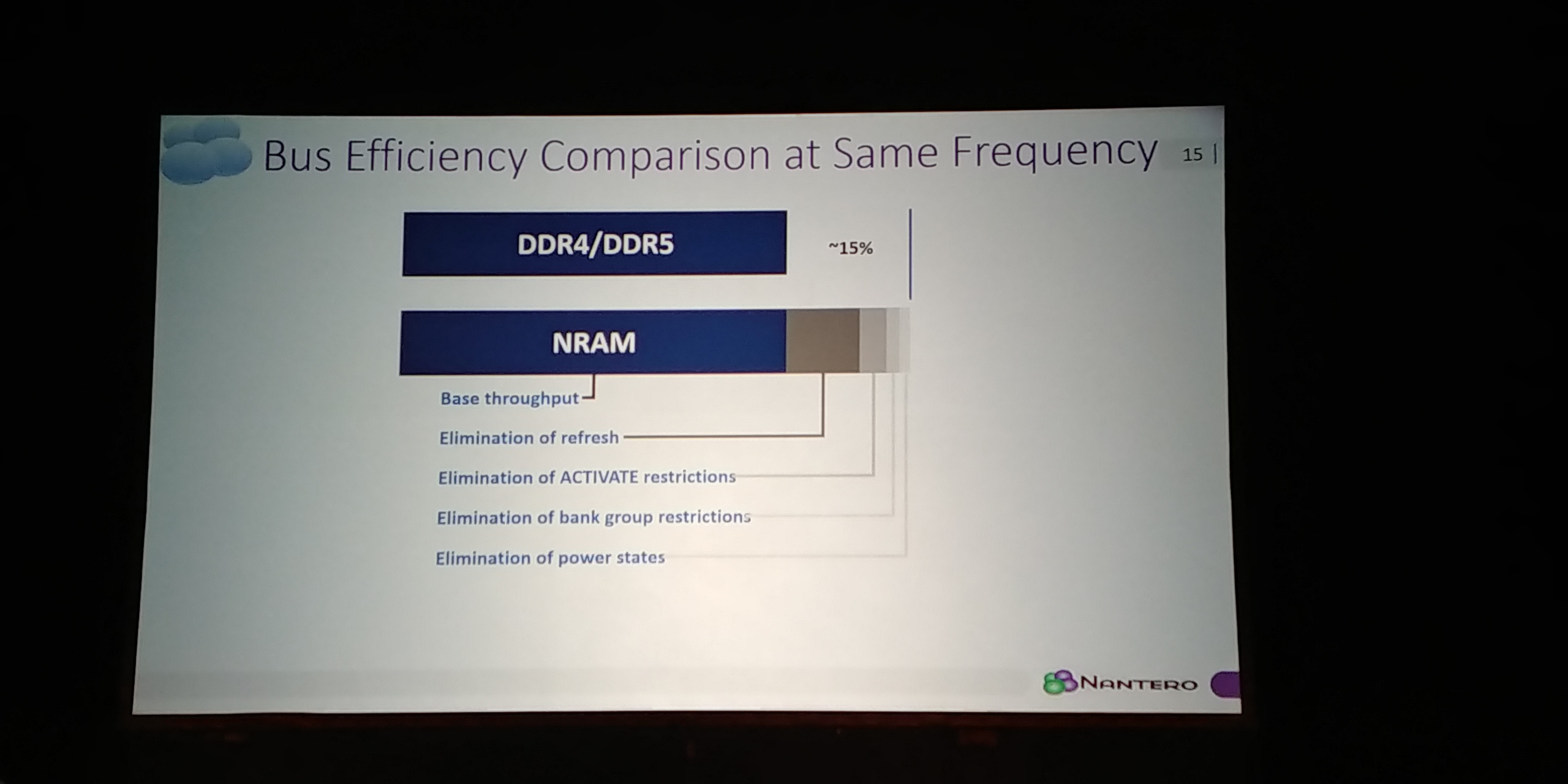
02:03PM EDT - So this is three grades of speed in DRAM terms
02:03PM EDT - Can build standard memory modules. They just work
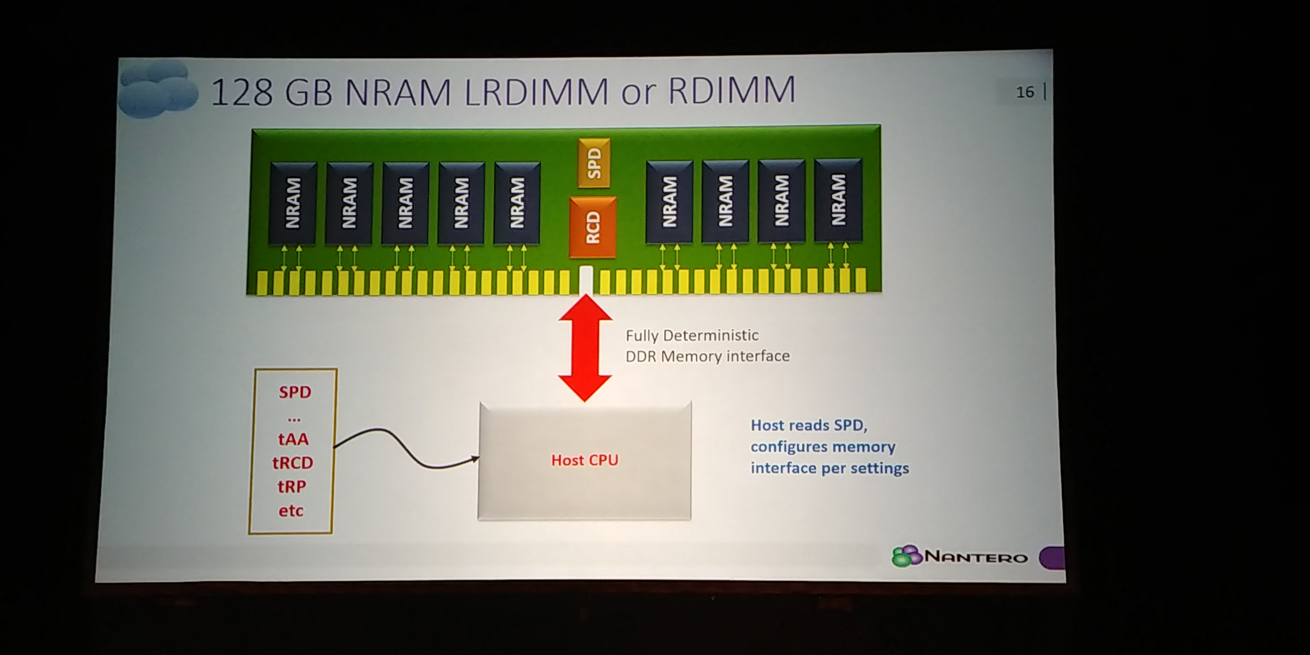
02:04PM EDT - 128GB NRAM LRDIMM or RDIMM

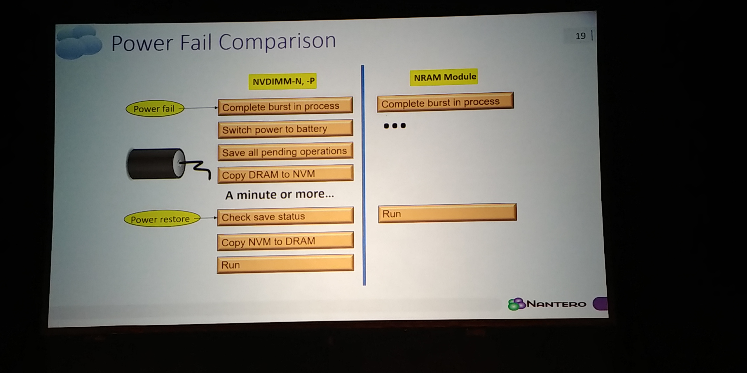
02:04PM EDT - For comparison, persistence memory through NVDIMM-N. Enables flash and power supply
02:04PM EDT - Requires buffers
02:04PM EDT - Half-DRAM and Half-Flash
02:05PM EDT - shutdown and startup time could be two minutes on NVDIMM-N
02:05PM EDT - NVDIMM-P is similar, but still non-deterministic

02:05PM EDT - Still need power, buffers
02:06PM EDT - Persistent memory such as NRAM means no reloading on power fail
02:06PM EDT - or limited
02:06PM EDT - helps with uptime
02:06PM EDT - Today, power fail means checkpointing reload. NRAM doesn't need that
02:07PM EDT - Persistent memory is becoming more aware in software
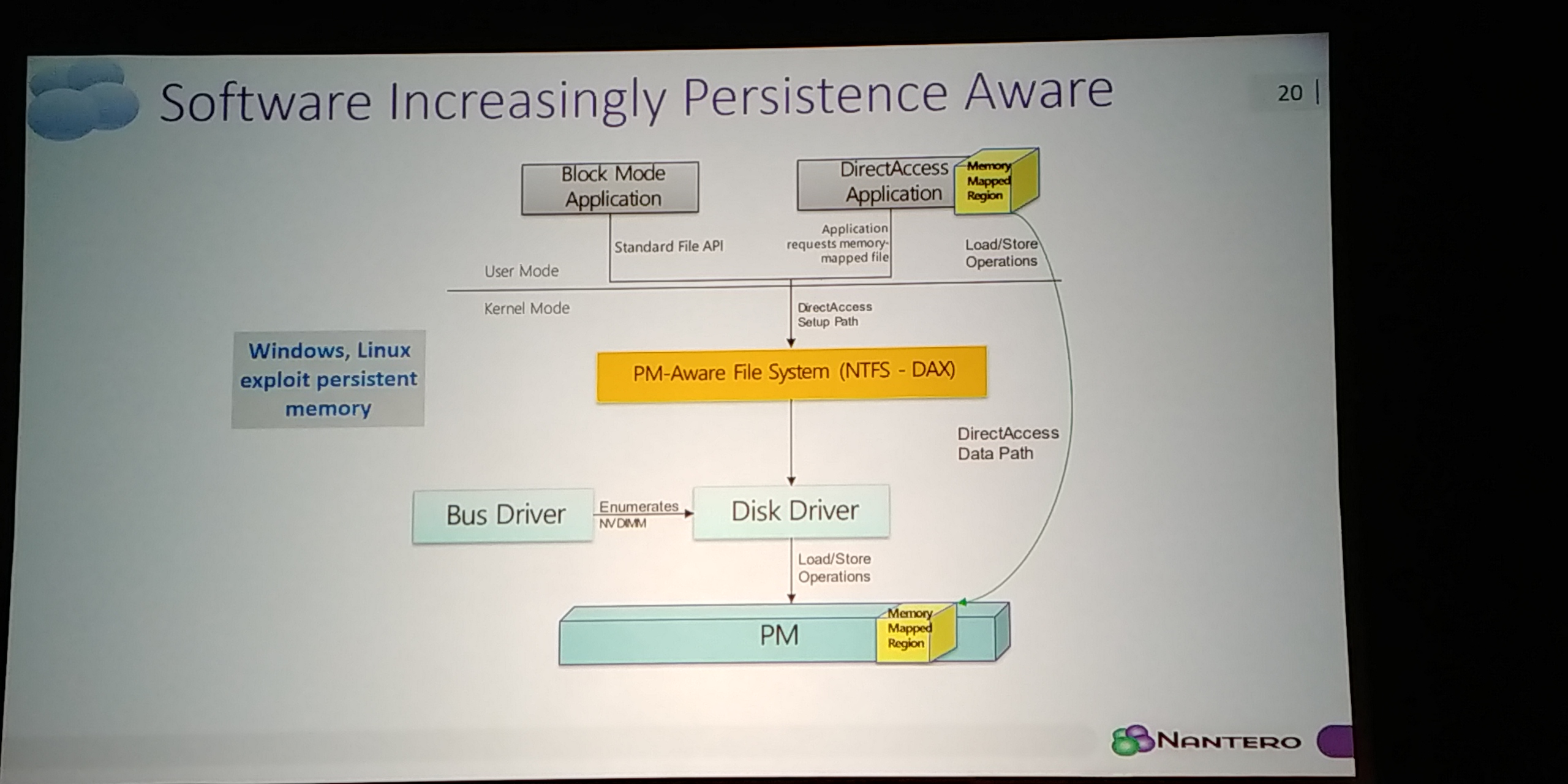
02:07PM EDT - Persistent memory aware file systems and such
02:08PM EDT - All blocks and procedures are available for licencing
02:08PM EDT - Can be incorporated directly into silicon
02:08PM EDT - DRAM compatible front end possible
02:08PM EDT - On-the-fly ECC
02:09PM EDT - unlimited write endurance
02:09PM EDT - Memory-Class Storage
02:09PM EDT - Industry is ready
02:09PM EDT - Additional performance in DRAM mode
02:09PM EDT - Scaling in both stacks and process nodes
02:09PM EDT - Q&A Time
02:11PM EDT - Q: What you talk about is almost too good to be true. What am I missing? A: It does not go well with Peanut Butter or salsa. But seriously, we've built 1000s of test chips and we have profiled them. We haven't built 16 Gb device yet, it's up to the customer. Maybe it's that 300C limit that's the downside.
02:12PM EDT - Q: Do you have a metric for approximate energy per bit? A: I should have included it. Power conusmption has a major ripple effect. It runs off of the same power supplies, with the same or less energy as DRAM. 5 femto-joule per bit activation
02:13PM EDT - Q: A lot of data from individual die. Data over a large sample? A: We chose to pull single cell because it's more readable. The accumulated data on the 5ns access time, that was over billions of cycles on billions of devices.
02:16PM EDT - Q: NVM device, but haven't said about security? Encryption? Otherwise it's not a drop-in. A: We have these conversations with customers, We're an IP house - we do chip design. We had those discussions about each chip has encyption, but for the mainstream device, much like the NVDIMM-N, it's up to the system guys. The strong message we have from customers is to not screw with it - they'll deal with it. THey want dumb simple memory chips and their own security.
02:16PM EDT - Q: Alpha particle rate? A: These devices have been sent into space. We know about extremes, radiation. Nothing can you do to a nanotube to do something weird. We have electrostatic protection, nothing else seems to affect it.
02:18PM EDT - Q: You said nothing about the hammer to write the system. Said about alignment, but A: It's a complex formulation, some under NDA. We can discuss about the nanotube selection - part of our secret source is about the CNT slurry. We build that and licence that - they use our proprietary technology to do nanotube selection. Tuned to the cell, the length and diameter has be tuned.
02:19PM EDT - Q: How do you flip it? A: Electrostatics. Voltage across a word line, a bit line, we have some proprietary technology to prevent sneak. Writes are faster than reads because you just throw it down the line.
02:19PM EDT - Q: When do you thin we can install these devices in these systems? 2018? 2019? 2020? A: 2-3 weeks ago Fujitsu announced they were taking CNT to mass market. So you can buy those next year or the year after. It's all about fabrication and testing.
02:20PM EDT - That's a wrap. A super interesting talk for sure. The next live blog is at 2pm PT about Arm's Machine Learning Core.


19 Comments
View All Comments
plopke - Tuesday, August 21, 2018 - link
I am not smart enough to understand all this but can i condlude1)they will only license the technology not make it themself
2)It scales less well in size than Intel Optane but is as fast RAM and is persistence?
Still i loved this article xD!
Arnulf - Wednesday, August 22, 2018 - link
1: It would appear so. Not a bad thing either, foundry business is extremely expensive.2: Quite the contrary, should scale really well due to the way each cell is constructed. Past that it's just a matter of implementing the front-end (which is no different than doing so for DRAM for example).
zapshere01 - Monday, December 31, 2018 - link
Remember that CNT's are discreet elements, and as such, have a fixed size (though small). These are likely MW tubes so are not nearly as small as SW tubes. Also, I imagine that to create and open current paths (plural is important) involves multiple tubes and paths. As such, statistics will play a role in the resistance of the on state, so with scaling, one might assume that fewer paths will be available and enabled, and as such, more variability in the on (and possibly off) state resistance. This will not only impact sensing of the on/off state at lower supply voltages, but also close the door on the possibility of multi-bit storage in a single cell. I'm not convinced that scaling is a slam dunk at all.Qwertilot - Tuesday, August 21, 2018 - link
Fun :) Potentially a lot of it if it can manufacture at any sort of speed.Can’t help but think they musn’t be trying hard enough when they claim ‘unlimited’ endurance!
Gunbuster - Tuesday, August 21, 2018 - link
Is it 2001? Those people need to drop some coin on a professional website and PowerPoint deck make over.RandomUsername3245 - Tuesday, August 21, 2018 - link
In my experience, flashy PPT themes are not taken seriously at technical conferences. People assume it's either marketing material with no technical depth or it's there to distract you from some other lack of content.p.s. very cool technology; hope to see it soon
Ian Cutress - Tuesday, August 21, 2018 - link
Correct. Simple slides are the best. It's for engineers, not marketing.wumpus - Tuesday, August 21, 2018 - link
Is the "300C limit" temperature? I think that's beyond automotive grade, but they seem impressive.I'd assume nanotube production would be an issue, but probably not. Scaling in size vs. Optane isn't all that much of an issue: expect the road to <5nm to be *slow*.
I'm curious why persistence is in such: I'd assume that [data corrupting] software and even hardware issues should be vastly more common than power issues. And it shouldn't be that hard to make a motherboard that can boot without clearing ram for the software issues.
But I want RAM cheaper than DRAM. Anybody know what the odds of this company being bought by Intel and this tech being quietly smothered? Cheap memory (i.e. DRAM, one of Intel's biggest inventions) helped microcomputers kill the minicomputer and mainframe, and even cheaper DRAM threatens Wintel (and Lintel) as once you need "real" amounts of memory, you can't justify putting a lower performance chip than high end x86 (ok, sometimes that means AMD, but you know what I mean).
Ian Cutress - Tuesday, August 21, 2018 - link
300C limit means at 300 Celsius, data retention goes down from 12000 years to 300 years.Dr. Swag - Wednesday, August 22, 2018 - link
Looks like optane might have some solid competition! :D