SK Hynix Publishes First Info on HBM3E Memory: Ultra-wide HPC Memory to Reach 8 GT/s
by Anton Shilov on May 30, 2023 7:00 AM EST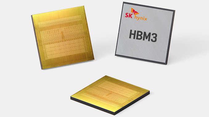
SK Hynix was one of the key developers of the original HBM memory back in 2014, and the company certainly hopes to stay ahead of the industry with this premium type of DRAM. On Tuesday, buried in a note about qualifying the company's 1bnm fab process, the the manufacturer remarked for the first time that it is working on next-generation HBM3E memory, which will enable speeds of up to 8 Gbps/pin and will be available in 2024.
Contemporary HBM3 memory from SK Hynix and other vendors supports data transfer rates up to 6.4Gbps/pin, so HBM3E with an 8 Gbpis/pin transfer rate will provide a moderate, 25% bandwidth advantage over existing memory devices.
To put this in context, with a single HBM stack using a 1024-bit wide memory bus, this would give a known good stack die (KGSD) of HBM3E around 1 TB/sec of bandwidth, up from 819.2 GB/sec in case of HBM3 today. Which, with modern HPC-class processors employing half a dozen stacks (or more), would work out to several TB/sec of bandwidth for those high-end processors.
According to the company's note, SK Hynix intends to start sampling its HBM3E memory in the coming months, and initiate volume production in 2024. The memory maker did not reveal much in the way of details about HBM3E (in fact, this is the first public mention of its specifications at all), so we do not know whether these devices will be drop-in compatible with existing HBM3 controllers and physical interfaces.
| HBM Memory Comparison | ||||||
| HBM3E | HBM3 | HBM2E | HBM2 | |||
| Max Capacity | ? | 24 GB | 16 GB | 8 GB | ||
| Max Bandwidth Per Pin | 8 Gb/s | 6.4 Gb/s | 3.6 Gb/s | 2.0 Gb/s | ||
| Number of DRAM ICs per Stack | ? | 12 | 8 | 8 | ||
| Effective Bus Width | 1024-bit | |||||
| Voltage | ? | 1.1 V | 1.2 V | 1.2 V | ||
| Bandwidth per Stack | 1 TB/s | 819.2 GB/s | 460.8 GB/s | 256 GB/s | ||
Assuming SK hynix's HBM3E development goes according to plan, the company should have little trouble lining up customers for even faster memory. Especially with demand for GPUs going through the roof for use in building AI training and inference systems, NVIDIA and other processor vendors are more than willing to pay premium for advanced memory they need to produce ever faster processors during this boom period in the industry.
SK Hynix will be producing HBM3E memory using its 1b nanometer fabrication technology (5th Generation 10nm-class node), which is currently being used to make DDR5-6400 memory chips that are set to be validated for Intel’s next generation Xeon Scalable platform. In addition, the manufacturing technology will be used to make LPDDR5T memory chips that will combine high performance with low power consumption.
Source: SK hynix


5 Comments
View All Comments
rpg1966 - Tuesday, May 30, 2023 - link
This might sound flippant, but why does the industry talk about performance of "known good stack dies"? What's the alternative, measuring performance of dies that failed in the production process?Amandtec - Tuesday, May 30, 2023 - link
I speculate - different dies can produce different grades of silicon - in this case 10Gbs vs 8Gbs.Kevin G - Tuesday, May 30, 2023 - link
Not all the dies in a stack will connect correctly. That is why nVidia's special H100 accelerators for ChatGPT have 94 GB of memory enabled instead of the 96 GB that is physically on the module. Two dies between the six stacks don't pass testing and are disabled. Maximum bandwidth figures are advertised with a fully functional stack. The reason for partially functional stacks is that leveraging through silicon vias (TSV) is tricky and there are well over two thousand vias per stack. With products like nVidia's H100, there are six stacks of HBM which also have to connect to the H100 die. That means a ~24,000 points of failure in packaging between the H100 and memory bus.Shaunathan - Tuesday, May 30, 2023 - link
kevin you smart i like yourpg1966 - Tuesday, May 30, 2023 - link
Thanks!