AMD Announces Zen 5-based EPYC “Turin” Processors: Up to 192 Cores, Coming in H2’2024
by Ryan Smith on June 3, 2024 1:15 PM EST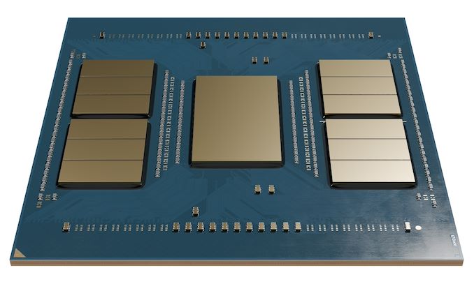
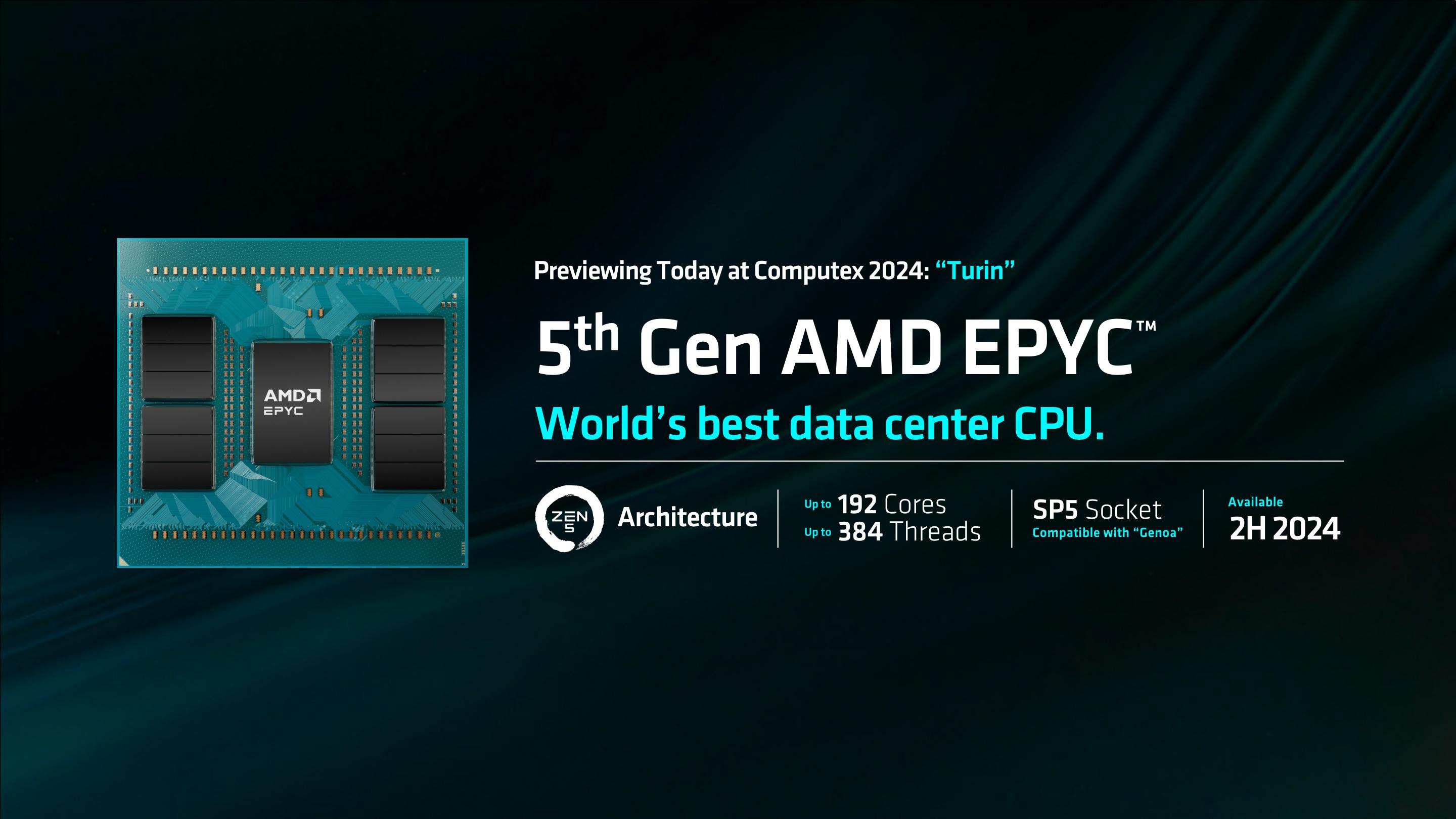
With AMD’s Zen 5 CPU architecture only a month away from its first product releases, the new CPU architecture was placed front and center for AMD’s prime Computex 2024 keynote. Outlining how Zen 5 will lead to improved products across AMD’s entire portfolio, the company laid out their product plans for the full triad: mobile, desktop, and servers. And while server chips will be the last parts to be released, AMD also saved the best for last by showcasing a 192 core EPYC “Turin” chip.
Turin is the catch-all codename for AMD’s Zen 5-based EPYC server processors – what will presumably be the EPYC 9005 series. The company has previously disclosed the name in earnings calls and other investor functions, outlining that the chip was already sampling to customers and that the silicon was “looking great.”
The Computex reveal, in turn, is the first time that the silicon has been shown off to the public. And with it, we’ve received the first official confirmation of the chip’s specifications. With SKUs up to 192 CPU cores, it’s going to be a monster of an x86 CPU.
| AMD EPYC CPU Generations | ||||
| AnandTech | EPYC 5th Gen (Turin, Z5c) |
EPYC 9704 (Bergamo) |
EPYC 9004 (Genoa) |
EPYC 7003 (Milan) |
| CPU Architecture | Zen 5c | Zen 4c | Zen 4 | Zen 3 |
| Max CPU Cores | 192 | 128 | 96 | 64 |
| Memory Channels | 12 x DDR5 | 12 x DDR5 | 12 x DDR5 | 8 x DDR4 |
| PCIe Lanes | 128 x 5.0 | 128 x 5.0 | 128 x 5.0 | 128 x 4.0 |
| L3 Cache | ? | 256MB | 384MB | 256MB |
| Max TDP | 360W? | 360W | 400W | 280W |
| Socket | SP5 | SP5 | SP5 | SP3 |
| Manufacturing Process |
CCD: TSMC N3 IOD:TSMC N6 |
CCD: TSMC N5 IOD: TSMC N6 |
CCD: TSMC N5 IOD: TSMC N6 |
CCD: TSMC N7 IOD: GloFo 14nm |
| Release Date | H2'2024 | 06/2023 | 11/2022 | 03/2021 |
Though only a brief tease, AMD’s Turin showcase did confirm a few, long-suspected details about the platform. AMD will once again be using their socket SP5 platform for Turin processors, which means the chips are drop-in compatible with EPYC 9004 Genoa (and Bergamo). The reuse of SP5 means that customers and server vendors can immediately swap out chips without having to build/deploy whole new systems. It also means that Turin will have the same base memory and I/O options as the EPYC 9004 series: 12 channels of DDR5 memory, and 128 PCIe 5.0 lanes.
In terms of power consumption, existing SP5 processors top out at 400 Watts, and we’d expect the same for these new, socket-compatible chips.
As for the Turin chip itself, while AMD is not going into further detail on its configuration, all signs point to this being a Zen 5c configuration – that is, built using CCDs designed around AMD’s compact Zen 5 core configuration. This would make the Turin chip on display the successor to Bergamo (EPYC 9704), which was AMD’s first compact core server processor, using Zen 4c cores. AMD’s compact CPU cores generally trade off per-core performance in favor of allowing more CPU cores overall, with lower clockspeed limits (by design) and less cache memory throughout the chip.
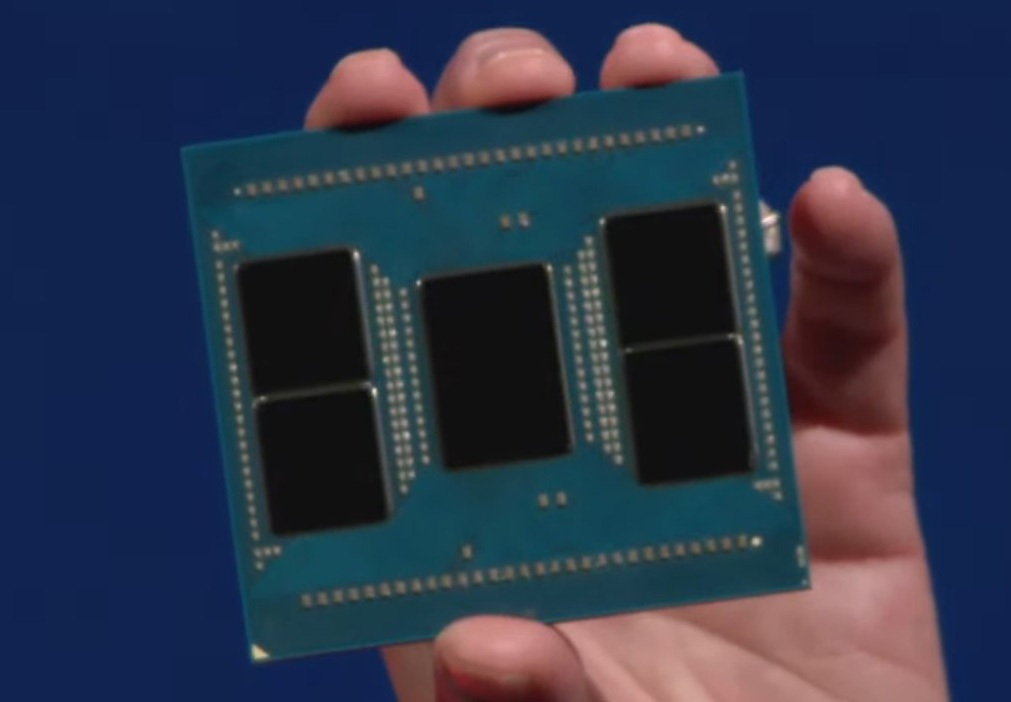
According to AMD, the CCDs on this chip were fabbed on a 3nm process (undoubtedly TSMC’s), with AMD apparently looking to take advantage of the densest process available in order to maximize the number of CPU cores the can place on a single chip. Even then, the CCDs featured here are quite sizable, and while we’re waiting for official die size numbers, it would come as no surprise if Zen 5’s higher transistor count more than offset the space savings of moving to 3nm. Still, AMD has been able to squeeze 12 CCDs on to the chip – 4 more than Bergamo – which is what’s allowing them to offer 192 CPU cores instead of 128 as in the last generation.
Meanwhile, the IOD is confirmed to be produced on 6nm. Judging from that fact, the pictures, and what AMD’s doing with their Zen 5 desktop products, there is a very good chance that AMD is using either the same or a very similar IOD as on Genoa/Bergamo. Which goes hand-in-hand with the socket/platform at the other end of the chip staying the same.
AMD’s brief teaser did not discuss at all any other Turin configurations. So there is nothing else official to share about Turin chips built using full-sized Zen 5 CPU cores. With that said, we know that the full-fat cores going into the Ryzen 9000 desktop series pack 8 cores to a CCD and are being fabbed on a 4nm process – not 3nm – so that strongly implies that EPYC Zen 5 CCDs will be the same. Which, if that pans out, means that Turin chips using high performance cores will max out at 96 cores, the same as Genoa.
Hardware configurations aside, AMD also showcased a couple of benchmarks, pitting the new EPYC chips against Intel’s Xeons. As you’d expect in a keynote teaser, AMD was winning handily. Though it is interesting to note that the chips benchmarked were all 128 core Turins, rather than on the 192 core model being shown off today.
AMD will be shipping EPYC Turin in the second half of this year. More details on the chips and configurations will follow once AMD gets closer to the EPYC launch.


29 Comments
View All Comments
Kevin G - Monday, June 3, 2024 - link
AMD is holding back here a bit. If the IO die is shared across Turin models (which was the same between Genoa and Bergamo), there are 16 Infinity Fabric links for Turin's IO die. In the picture there are only 12 processor chiplets with 16 cores each to get to 192 cores. However, AMD's 128 core part is built around 16 chiplets with 8 cores each. There is physical room to fit four additional dies and the Infinity Fabric links are there for a potential 256 core part.Speaking of the IO die, this one is huge. Off hand it appears to be even larger than the one used in Genoa/Bergamo. Only surprise here is that AMD hasn't moved to 136 PCIe 5.0 lanes instead of the previous 128 PCIe 5.0 + 8 lanes of PCIe 3.0. My presumption is that the lanes meant for IPMI and service tasks would be getting a bandwidth boost. Likely a bit too early for disclosure, but what levels and version of CXL is supported is also expected to be greater than Genoa/Bergamo.
The Von Matrices - Monday, June 3, 2024 - link
I doubt that is the main reason. Each Zen4 chiplet can use 2 IF links, so the 12 chiplet models actually lose half their interface bandwidth compared to the 8 chiplet models. How much performance loss is debatable but the main reason for 16 links was always to have dual links for each chiplet when possible, not to have 16 chipletsKevin G - Tuesday, June 4, 2024 - link
True but with Zen 4 Genoa, running dual Infinity Fabric links was only possible with the Epyc IO die with 4 chiplets or less due to how the links are partitioned internally on the IO die. There are 12 links available arranged in sets of three tied to a six by 32 bit DDR5 memory controller in a chip's quadrants. Oddball rule but you can't have a CCD split across two of the internal quadrants However to my knowledge, AMD never leverage dual links to Zen 4 dies in any shipping product: it was more cost effective to do design/test/validate/mass manufacture only handful of interposers and selectively populate dies on them. For example, a 48 core part would have four pads empty where two more dies could be added to make it a 64 core part. Essentially 8 chiplets and below + IO die got one interposer design while the 96 core part and Bergamo got their own specialized interposers.AMD has done something similar with AM5 Zen 4 parts as there is a spot on the interposer where a second die could go on the 8 core and less models. It has been my impression that AMD's consumer IO die for AM5 also supports running dual link to a single CCD but they haven't leveraged it in shipping products for identical testing/economies of scale reasoning.
This new IO die increases link count so running up to 8 chiplets with dual Infinity Fabric links is on the table. It'll be interesting to see if AMD flexes their options more with Zen 5 as the focus has been on latency and bandwidth.
dotjaz - Friday, July 26, 2024 - link
Direct quote from AMD."In processor models
with four CPU dies, two connections can be used to optimize
bandwidth to each CPU die. This is the case for some EPYC 9004
Series CPUs and all EPYC 8004 Series CPUs"
dotjaz - Friday, July 26, 2024 - link
https://www.amd.com/system/files/documents/4th-gen...Kaique Gerais - Friday, June 7, 2024 - link
Where are you getting 16 Chiplets from? 12 ccd by all information is the maximum amountdotjaz - Friday, July 26, 2024 - link
There are 16 IF links, therefore up to 16 CCX is possible, maybe not on SP5 due to routing, but it is possible.NextGen_Gamer - Monday, June 3, 2024 - link
I wouldn't presume that the Zen 5 (non-C) version is built using TSMC N4. It is probable, yes, but on the mobile side "Strix Point" is a combination of Zen 5/Zen 5C and using TSMC N4. That means AMD already took the time to design Zen 5C around both TSMC N4 and N3 nodes, releasing in the same year even. It wouldn't be a stretch to say they did the same for Zen 5, especially being that EPYC is much more profitable than Ryzen.Kaique Gerais - Friday, June 7, 2024 - link
So as far as i understand Zen C cores are developed from mobile, so if next generation APU is being designed on 3nm it would make sense for zen 5c to have both 4nm and 3nm where as big Zen 5 is only on 4nm.ballsystemlord - Monday, June 3, 2024 - link
A real pity we only got a NAMD benchmark for regular computing applications.