Samsung and TSMC Roadmaps: 8 and 6 nm Added, Looking at 22ULP and 12FFC
by Anton Shilov on May 5, 2017 9:30 AM ESTNot Everyone Needs Leading Edge: TSMC’s 22 nm ULP, 12 nm FFC and 12 nm FFC+
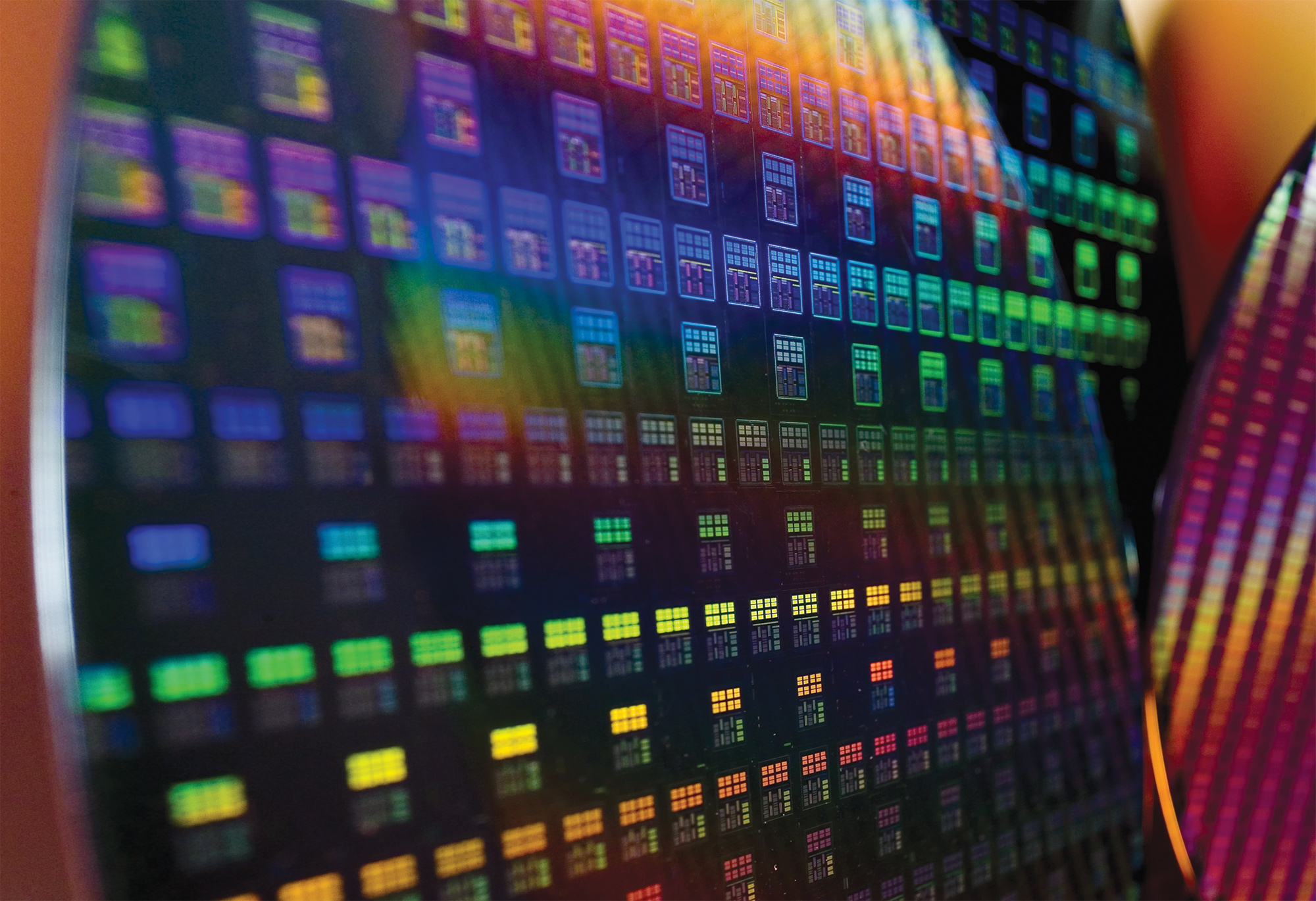
Now let’s discuss something less advanced, but what is required for hundreds of millions of devices sold every year.
| Advertised PPA Improvements of TSMC's Low-Power/Compact Nodes Data announced by TSMC during conference calls, press briefings and in press releases |
||||||||
| CLN28HPC vs CLN28HPM |
CLN28HPC+ vs CLN28HPM |
CLN22LPU vs CLNHPC+ |
CLN16FFC vs CLN16FF |
CLN12FFC vs CLN16FFC |
12FFC-ULP vs CLN12FFC |
|||
| Power | 20% | 30% | 35% | lower | 25% | lower | ||
| Performance | - | 15% | 15% | unknown | 10% | unknown | ||
| Area Reduction | 10% | 10% | 10% | optional | 20% | unknown | ||
| HVM Start | started | started | 2018 | Q1 2016 | 2018 | 2019 | ||
| Note | Planar 28 nm-based |
FinFET 16/20 nm-based |
||||||
Development of FinFET-based chips is more expensive of ICs featuring planar transistors and their manufacturing is more costly as well. As a result, FinFET is virtually unavailable for many smaller designers of SoCs that usually build various solutions for emerging IoT applications. GlobalFoundries and Samsung offer their FD-SOI manufacturing processes to such companies (and these technologies have a number of other advantages in addition to being more cost-effective), whereas TSMC intends to introduce its new 22 nm ULP technology aimed at such applications. The CLN22ULP is an optimized version of the company’s 28 nm HPC+ (high-performance compact plus) manufacturing process that has been available for a while. The 22ULP offers a 10% area reduction and either a 15% performance improvement over the 28HPC+ process, or a 35% power drop. The 22ULP process joins a family of other ultra-low-power processes offered by TSMC and will compete against GlobalFoundries 22FDX as well as Samsung’s 28 nm FD-SOI offering.
Next up is TSMC’s 12 nm FFC manufacturing technology, which is an optimized version of the company’s CLN16FFC that is set to use 6T libraries (as opposed to 7.5T and 9T libraries) providing a 20% area reduction. Despite noticeably higher transistor density, the CLN12FFC is expected to also offer a 10% frequency improvement at the same power and complexity or a 25% power reduction at the same clock rate and complexity. Further down the road, TSMC also plans to offer a ULP version of the CLN12FFC with reduced voltage, but that is going to happen only in 2018 or 2019.
Sources: Samsung, TSMC, SemiWiki (1, 2, 3).
Related Reading:
- Samsung Foundry Announces 10nm SoC In Mass-Production
- Samsung Announces Second-Gen 14nm Low Power Plus (14LPP) Process Now In Mass Production
- EUV Lithography Makes Good Progress, Still Not Ready for Prime Time
- GlobalFoundries to Expand Capacities, Build a Fab in China
- Intel to Equip Fab 42 for 7 nm
- GlobalFoundries Updates Roadmap: 7 nm in 2H 2018, EUV Sooner Than Later?


89 Comments
View All Comments
mdriftmeyer - Friday, May 5, 2017 - link
Being 63.63 times smaller in diameter for an atom compared to the fab process is quite a large span in scale.boeush - Saturday, May 6, 2017 - link
One thing to consider, though, is that when atoms are bound into molecules via covalent bonds, the distances between their nuclei shrink below the sum of the adjacent atoms' stand-alone radii: in other words, chemically bound atoms pack together much more tightly than one might naively expect by conceptualizing each atom as a solid sphere...Jon Tseng - Friday, May 5, 2017 - link
PSA: NODES WITH THE SAME (NUMERICAL) NAME FROM DIFFERENT VENDORS ARE NOT EQUIVALENT.Just wanted to get that out of the way early! :-p
Meteor2 - Friday, May 5, 2017 - link
Indeed. The x nm labels are meaningless now; they may as well call them Bob and Joan.The only way to compare them is via the inter-node PPA change metrics. Anyone have numbers for 22->14 and 14->10 from Intel to hand?
Even then I know Intel's 14 nm is better on at least power and performance than others' 14/16 nm, as the latter are actually 20 nm with FinFET added, but I'm not aware of any meaningful way of comparing them.
lefty2 - Friday, May 5, 2017 - link
That's not totally true. The first iteration of Intel's 14nm performed worse than TSMC's 16nm. 14nm+ is much better thoughDrumsticks - Friday, May 5, 2017 - link
I'm not calling you wrong or anything, but can you source that? Intel's original 14nm might have had bad yields for a while, but I imagine it's difficult to compare outright performance without published numbers, given that Intel's 14nm went into CPUs with a frequency of 800MHz to 4.5 GHz, versus TSMC's biggest wins being Apple and GPUs, none of which went past the low 2GHzs. Obviously it's difficult to compare performance on frequency with something like that.SuperMecha - Saturday, May 6, 2017 - link
See page 4. There are probably several other factors that determine performance other than leakage and drive current.https://newsroom.intel.com/newsroom/wp-content/upl...
Meteor2 - Sunday, May 7, 2017 - link
Good link, and a good quote within:"Industry “10 nm” technologies are expected to ship sometime in 2017 and have similar density to Intel’s 14 nm technology that has been shipping since 2014."
helvete - Thursday, July 20, 2017 - link
Would you expect anything else from Intel paper? (Not telling they are far from the truth)lefty2 - Saturday, May 6, 2017 - link
The first iteration of 14nm was Broadfield and Broadfield did not clock to 4.5GHz. Also, you can't compare to a smartphone SoC, which have to keep within a very small power envelope.