Samsung and TSMC Roadmaps: 8 and 6 nm Added, Looking at 22ULP and 12FFC
by Anton Shilov on May 5, 2017 9:30 AM ESTBeyond 10 nm at Samsung: 8 nm and 6 nm
Samsung’s 7 nm manufacturing technology is still expected to be the company’s first process to use extreme ultraviolet lithography (EUVL) for high-volume manufacturing (HVM) and that is going to happen sometimes in 2019 or later (risk production starts in the second half of 2018). In fact, the next several years down the road is where things will start to get interesting as Samsung announced another two new production technologies it has not talked about before: the 8 nm and the 6 nm processes.
| Industry FinFET Lithography Roadmap, HVM Start Data announced by companies during conference calls, press briefings and in press releases |
||||||||||||
| 2016 | 2017 | 2018 | 2019 | 2020 | 2021 | |||||||
| 1H | 2H | 1H | 2H | 1H | 2H | 1H | 2H | |||||
| GlobalFoundries | 14LPP | 7nm DUV | 7nm with EUV* | |||||||||
| Intel | 14 nm 14 nm+ |
14 nm++ 10 nm |
10 nm+ 10 nm++ |
|||||||||
| Samsung | 14LPP 14LPC |
10LPE | 10LPP | 8LPP 10LPU |
7LPP | 6 nm* (?) | ||||||
| SMIC | 28 nm** | 14 nm in development | ||||||||||
| TSMC | CLN16FF+ CLN16FFC | CLN10FF CLN16FFC |
CLN7FF CLN12FFC |
CLN12FFC/ CLN12ULP |
CLN7FF+ | 5 nm* (?) | ||||||
| UMC | 28 nm** | 14nm | no data | |||||||||
| *Exact timing not announced **Planar |
||||||||||||
Officially, Samsung says that both technologies will offer “greater scalability, performance and power advantages when compared to existing process nodes,” which obviously means that they are across the board better than Samsung’s current-gen 14 nm and 10 nm offerings. What is important is that Samsung also says that the “8 nm and the 6 nm will inherit all innovations from the latest 10 nm and the 7 nm technologies” respectively. This means that the 8 nm is set to keep using DUV and multi patterning (triple patterning or even quad patterning to be exact, but Samsung has not confirmed usage of the latter) for critical layers, whereas the 6 nm will come after 7 nm and will be Samsung’s second-generation EUV technology.
The only thing that Samsung confirms about its 8LPP manufacturing technology right now is the fact that this is a DUV-based process technology designed to shrink die size (i.e., increase transistor density) and frequency compared to the 10LPP fabrication process. Given the name of the technology and its key advertised advantages over direct predecessor, it is highly likely that the 8LPP will be used to make high-performance SoCs in 2019.
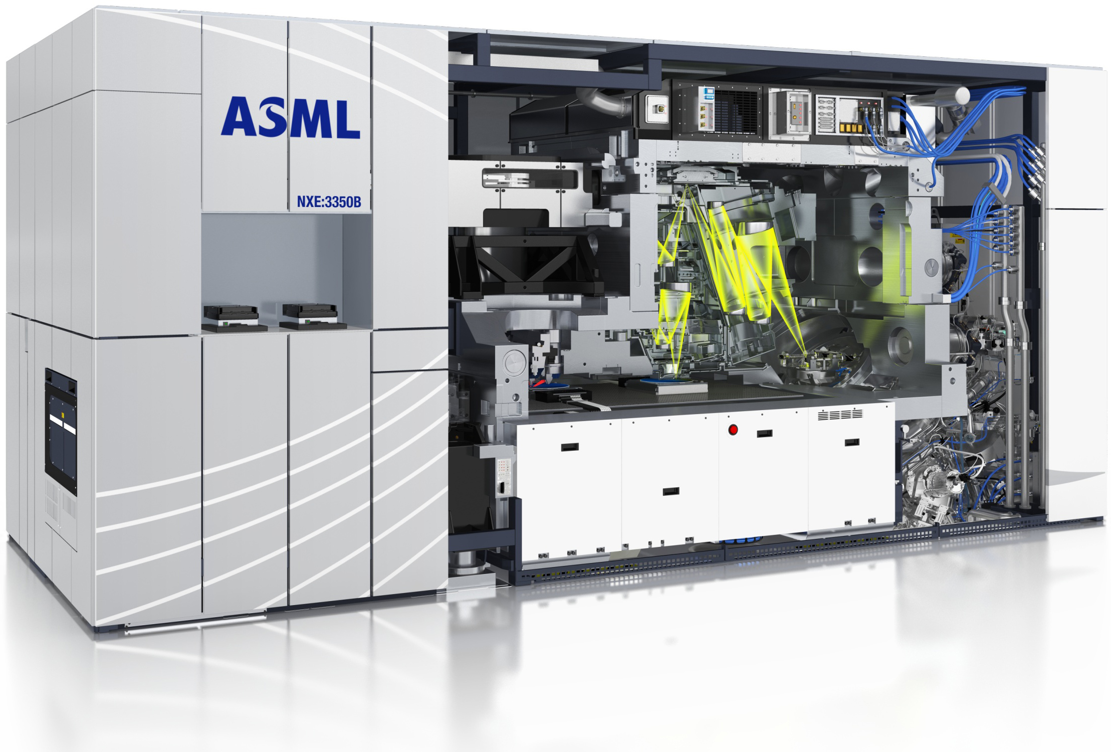
Since Samsung plans to start risk production using the 7LPP in the second half of 2018, the technology is hardly going to be used for high-volume manufacturing before the second half of 2019. Keeping in mind that Samsung now begins HVM using its leading-edge process technologies in October, it is possible that it is going to kick-off 7LPP HVM in fall 2019, but the 8LPP will be Samsung’s most advanced process technology for the better part of the year. Samsung does not mention timeframes for its 6 nm process technology and what to expect from it, but it is logical to assume that it will require more layers to be processed using ASML's EUV tools (like the NXE:3350B pictured above) in a bid to provide PPA advantages and it not be used for high-volume manufacturing before late 2020.
In March, Samsung only made brief announcements regarding its 10LPU, 8LPP and 6 nm process technology without disclosing their exact specifications or even PPA improvements targets. The addition of at least two more DUV technologies (the 10LPU and the 8LPP) in general may indicate that EUV may not be the best choice for all applications in 2019 – 2021, which is perfectly logical. Then again, we do not know how DUV and EUV technologies will co-exist early in the EUV era.
We are going to learn more about Samsung’s plans in the foundry industry in late May, when the company hosts its 2017 U.S Samsung Foundry Forum. So, we will have to wait for a couple of months for Samsung to disclose the whole picture regarding its upcoming process technologies.


89 Comments
View All Comments
Azethoth - Friday, May 5, 2017 - link
This is exciting news. The existence of GigaFabs means we must be getting close to the first MegaFab!ishould - Friday, May 5, 2017 - link
You mean TeraFab?LuckyWhale - Tuesday, May 9, 2017 - link
I wish Anton would work more on his writing or get a better editor. He writes English so mechanically and itis painfully obvious English is nowhere near his first tongue. I used to follow him at Xbitlabs. Great content but poor writing! sorry.ABR - Thursday, May 11, 2017 - link
Hmm, normally I'm a stickler about this stuff but with Anton's articles I guess I'm usually so immersed in the content that I don't notice anything!nhisaka - Tuesday, May 9, 2017 - link
In lịch tết 2018 : http://thietkelichtet.vn/bang-gia-in-lich-tet-bang...Thiet ke biet thu: http://katahome.com/thiet-ke-biet-thu
darkich - Wednesday, May 10, 2017 - link
Soo..no 7nm on Intel's roadmap?Seems like Samsung, GF and TSMC are on their way to leave it in the dust
peevee - Friday, May 12, 2017 - link
The "nodes" are just pure lies at this point. 45nm doubled gate density of 65nm, as expected. 10nm chips should have 20 times more transistors per area unit compared to 45nm. They are not even close. And there is nothing which is really 10nm, even a feature as simple as metal pitch is 40-50nm.RubiNBA - Monday, May 15, 2017 - link
The NBA live mobile Online additionally help gamers earn coins that are easy and quick. Since the primary resources in the game is coins, players that have use of unlimited coins have better opportunity to win the game as well as at a short time that is considerable.
Source : http://ow.ly/AHwi30aK5bD
thuantruongadw - Saturday, July 22, 2017 - link
Đất nền Long Hưng https://khudothi-longhung.comKhu đô thị Long Hưng https://khudothi-longhung.com/tien-ich-khu-do-thi-...
Đất nền long hưng giá rẻ nên đầu tư ngay https://datnenvensong.info/